74VHC112 Dual J-K Flip-Flops with Preset and Clear
September 1995
Revised April 1999
74VHC112
Dual J-K Flip-Flops with Preset and Clear
General Description
The VHC112 is an advanced high speed CMOS device
fabricated with silicon gate CMOS technology. It achieves
the high-speed operation similar to equivalent Bipolar
Schottky TTL while maintaining the CMOS low power dissi-
pation.
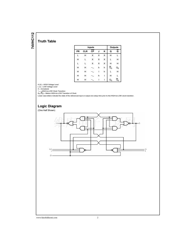
The VHC112 contains two independent, high-speed JK flip-
flops with Direct Set and Clear inputs. Synchronous state
changes are initiated by the falling edge of the clock. Trig-
gering occurs at a voltage level of the clock and is not
directly related to transition time. The J and K inputs can
change when the clock is in either state without affecting
the flip-flop, provided that they are in the desired state dur-
ing the recommended setup and hold times relative to the
falling edge of the clock. The LOW signal on PR or CLR
prevents clocking and forces Q and Q HIGH, respectively.
Simultaneous LOW signals on PR and CLR force both Q
and Q HIGH.
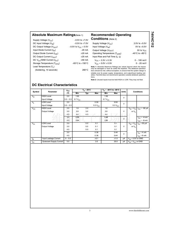
An input protection circuit ensures that 0V to 7V can be
applied to the input pins without regard to the supply volt-
age. This device can be used to interface 5V to 3V systems
and two supply systems such as battery backup. This cir-
cuit prevents device destruction due to mismatched supply
and input voltages.
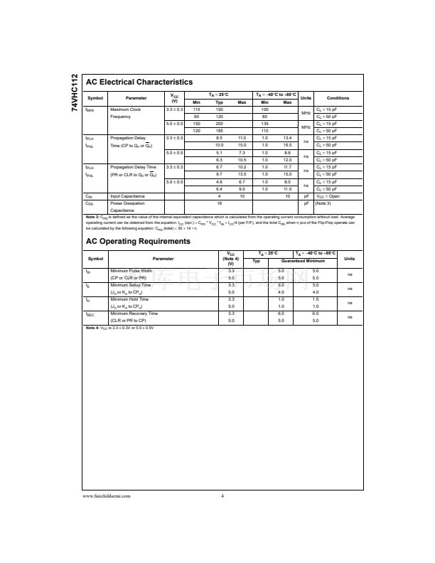
Features
s
High speed: f
MAX
= 200 MHz (typ) at V
CC
= 5.0V
s
Low power dissipation: I
CC
= 2
碌A
(max) at T
A
= 25掳C
s
High noise immunity: V
NIH
= V
NIL
= 28% V
CC
(min)
s
Power down protection is provided on all inputs
s
Pin and function compatible with 74HC112
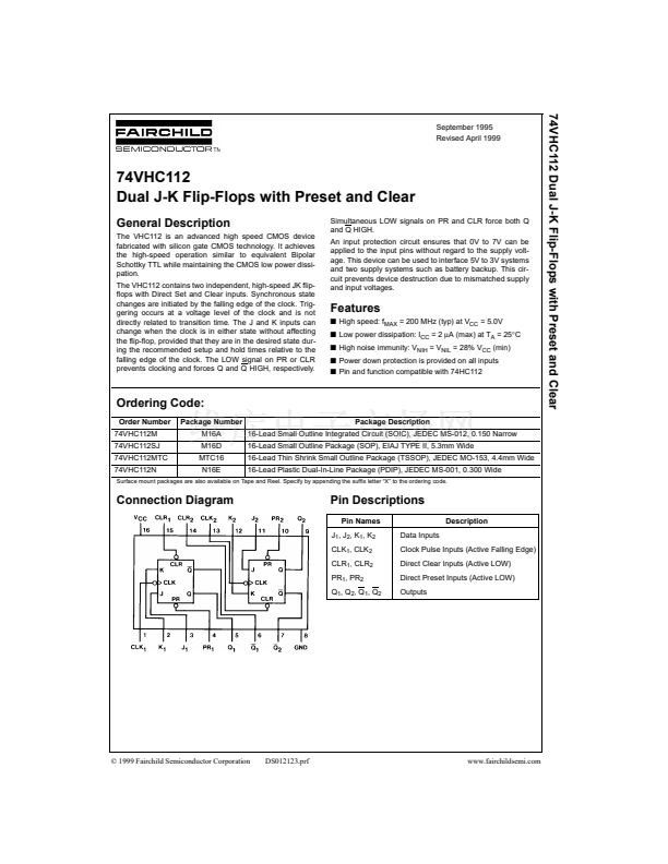
Ordering Code:
Order Number
74VHC112M
74VHC112SJ
74VHC112MTC
74VHC112N
Package Number
M16A
M16D
MTC16
N16E
Package Description
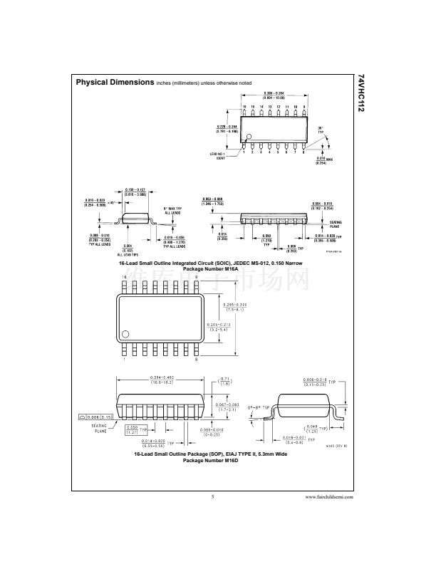
16-Lead Small Outline Integrated Circuit (SOIC), JEDEC MS-012, 0.150 Narrow
16-Lead Small Outline Package (SOP), EIAJ TYPE II, 5.3mm Wide
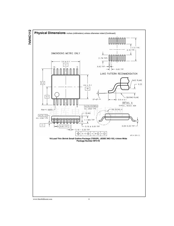
16-Lead Thin Shrink Small Outline Package (TSSOP), JEDEC MO-153, 4.4mm Wide
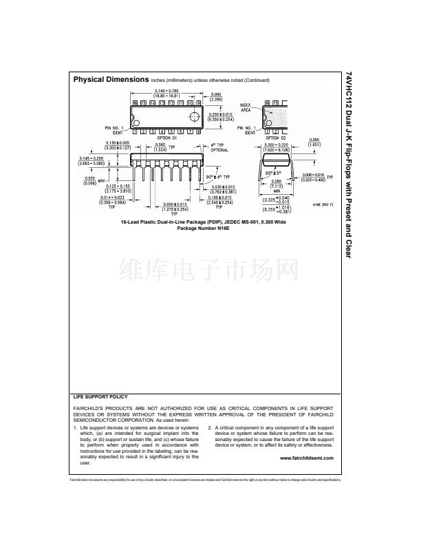
16-Lead Plastic Dual-In-Line Package (PDIP), JEDEC MS-001, 0.300 Wide
Surface mount packages are also available on Tape and Reel. Specify by appending the suffix letter 鈥淴鈥?to the ordering code.
Connection Diagram
Pin Descriptions
Pin Names
J
1
, J
2
, K
1
, K
2
CLK
1
, CLK
2
CLR
1
, CLR
2
PR
1
, PR
2
Q
1
, Q
2
, Q
1
, Q
2
Data Inputs
Clock Pulse Inputs (Active Falling Edge)
Direct Clear Inputs (Active LOW)
Direct Preset Inputs (Active LOW)
Outputs
Description
漏 1999 Fairchild Semiconductor Corporation
DS012123.prf
www.fairchildsemi.com


 1
1
 2
2
 3
3
 4
4
 5
5
 6
6
 7
7
