鈥?/div>
鈥?Low-cost, Easy-to-use Software Tools
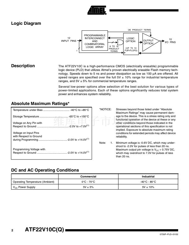
High-speed, Electrically Erasable Programmable Logic Devices
鈥?5 ns Maximum Pin-to-pin Delay
CMOS- and TTL-compatible Inputs and Outputs
鈥?Latch Feature Holds Inputs to Previous Logic States
Pin-controlled Standby Power (10 碌A Typical)
Advanced Flash Technology
鈥?Reprogrammable
鈥?100% Tested
High-reliability CMOS Process
鈥?20-year Data Retention
鈥?100 Erase/Write Cycles
鈥?2,000V ESD Protection
鈥?200 mA Latch-up Immunity
Dual Inline and Surface Mount Packages in Standard Pinouts
PCI-compliant
True Input Transition Detection 鈥淶鈥?and 鈥淨Z鈥?Version
鈥?/div>
鈥?/div>
鈥?/div>
High-
performance
EE PLD
ATF22V10C
ATF22V10CQ
See separate datasheet
for ATF22V10CZ and
ATF22V10CQZ options.
24
23
22
21
20
19
18
17
16
15
14
13
VCC
I/O
I/O
I/O
I/O
I/O
I/O
I/O
I/O
I/O
I/O
IN
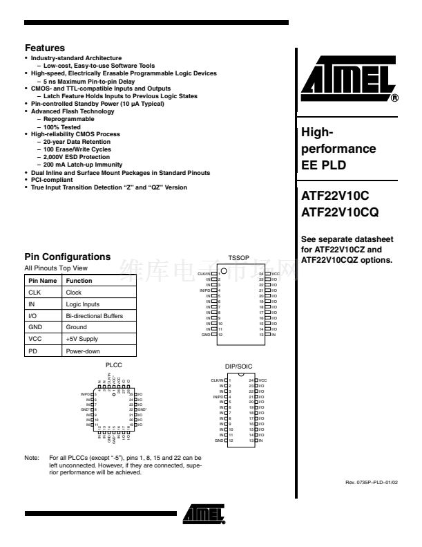
Pin Configurations
All Pinouts Top View
Pin Name
CLK
IN
I/O
GND
VCC
PD
Function
Clock
Logic Inputs
Bi-directional Buffers
Ground
+5V Supply
Power-down
PLCC
IN
IN
CLK/IN
VCC*
VCC
I/O
I/O
TSSOP
CLK/IN
IN
IN
IN/PD
IN
IN
IN
IN
IN
IN
IN
GND
1
2
3
4
5
6
7
8
9
10
11
12
DIP/SOIC
CLK/IN
IN
IN
IN/PD
IN
IN
IN
IN
IN
IN
IN
GND
1
2
3
4
5
6
7
8
9
10
11
12
24
23
22
21
20
19
18
17
16
15
14
13
VCC
I/O
I/O
I/O
I/O
I/O
I/O
I/O
I/O
I/O
I/O
IN
4
3
2
1
28
27
26
Note:
For all PLCCs (except 鈥?5鈥?, pins 1, 8, 15 and 22 can be
left unconnected. However, if they are connected, supe-
rior performance will be achieved.
Rev. 0735P鈥揚LD鈥?1/02
IN
IN
GND
GND*
IN
I/O
I/O
12
13
14
15
16
17
18
IN/PD
IN
IN
GND*
IN
IN
IN
5
6
7
8
9
10
11
25
24
23
22
21
20
19
I/O
I/O
I/O
GND*
I/O
I/O
I/O
1


 1
1
 2
2
 3
3
 4
4
 5
5
 6
6
 7
7
 8
8
 9
9
 10
10
 11
11
 12
12
 13
13
 14
14
 15
15
 16
16
 17
17
 18
18
