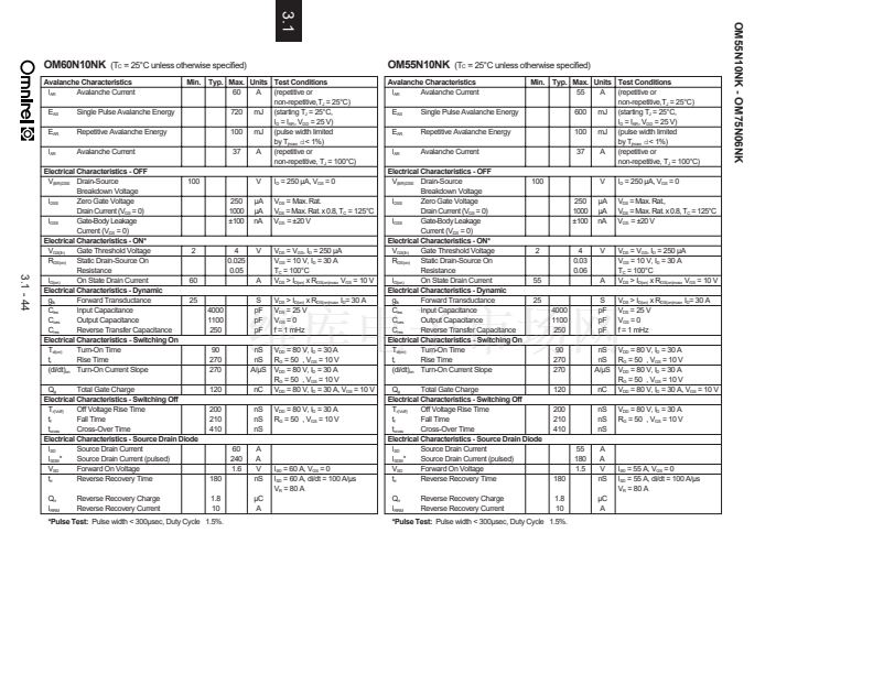
3.1
OM55N10NK - OM75N06NK
OM60N10NK
(T
C
= 25掳C unless otherwise specified)
Min. Typ. Max. Units Test Conditions
60
A
(repetitive or
non-repetitive,T
J
= 25掳C)
720 mJ (starting T
J
= 25掳C,
I
D
= I
AR
, V
DD
= 25 V)
100 mJ (pulse width limited
by T
jmax
,
d<
1%)
37
A
(repetitive or
non-repetitive, T
J
= 100掳C)
100
250
1000
卤100
V
碌A
碌A
nA
I
D
= 250 碌A, V
GS
= 0
V
DS
= Max. Rat.
V
DS
= Max. Rat. x 0.8, T
C
= 125掳C
V
GS
= 卤20 V
OM55N10NK
(T
C
= 25掳C unless otherwise specified)
Min. Typ. Max. Units Test Conditions
55
A
(repetitive or
non-repetitive,T
J
= 25掳C)
600 mJ (starting T
J
= 25掳C,
I
D
= I
AR
, V
DD
= 25 V)
100 mJ (pulse width limited
by T
jmax
,
d<
1%)
37
A
(repetitive or
non-repetitive, T
J
= 100掳C)
100
250
1000
卤100
V
碌A
碌A
nA
I
D
= 250 碌A, V
GS
= 0
V
DS
= Max. Rat.,
V
DS
= Max. Rat. x 0.8, T
C
= 125掳C
V
GS
= 卤20 V
Avalanche Characteristics
Avalanche Current
I
AR
E
AS
E
AR
I
AR
Single Pulse Avalanche Energy
Repetitive Avalanche Energy
Avalanche Current
Avalanche Characteristics
Avalanche Current
I
AR
E
AS
E
AR
I
AR
Single Pulse Avalanche Energy
Repetitive Avalanche Energy
Avalanche Current
Electrical Characteristics - OFF
V
(BR)DSS
Drain-Source
Breakdown Voltage
Zero Gate Voltage
I
DSS
Drain Current (V
GS
= 0)
Gate-Body Leakage
I
GSS
Current (V
DS
= 0)
Electrical Characteristics - ON*
Gate Threshold Voltage
V
GS(th)
R
DS(on)
Static Drain-Source On
Resistance
On State Drain Current
I
D(on)
Electrical Characteristics - Dynamic
Forward Transductance
g
fs
Input Capacitance
C
ies
Output Capacitance
C
oes
Reverse Transfer Capacitance
C
res
Electrical Characteristics - Switching On
Turn-On Time
T
d(on)
Rise Time
t
r
(di/dt)
on
Turn-On Current Slope
2
4
0.025
0.05
V
60
25
4000
1100
250
90
270
270
120
200
210
410
60
240
1.6
180
1.8
10
A
S
pF
pF
pF
V
DS
= V
GS
, I
D
= 250 碌A
V
GS
= 10 V, I
D
= 30 A
T
C
= 100掳C
V
DS
> I
D(on)
x R
DS(on)max
, V
GS
= 10 V
V
DS
> I
D(on)
x R
DS(on)max
, I
D
= 30 A
V
DS
= 25 V
V
GS
= 0
f = 1 mHz
Total Gate Charge
Q
g
Electrical Characteristics - Switching Off
Off Voltage Rise Time
T
r(Voff)
Fall Time
t
f
Cross-Over Time
t
cross
Electrical Characteristics - Source Drain Diode
Source Drain Current
I
SD
Source Drain Current (pulsed)
I
SDM
*
Forward On Voltage
V
SD
Reverse Recovery Time
t
rr
Q
rr
I
RRM
Reverse Recovery Charge
Reverse Recovery Current
nS V
DD
= 80 V, I
D
= 30 A
nS R
G
= 50 , V
GS
= 10 V
A/碌S V
DD
= 80 V, I
D
= 30 A
R
G
= 50 , V
GS
= 10 V
nC V
DD
= 80 V, I
D
= 30 A, V
GS
= 10 V
nS
nS
nS
A
A
V
nS
碌C
A
V
DD
= 80 V, I
D
= 30 A
R
G
= 50 , V
GS
= 10 V
Electrical Characteristics - OFF
V
(BR)DSS
Drain-Source
Breakdown Voltage
Zero Gate Voltage
I
DSS
Drain Current (V
GS
= 0)
Gate-Body Leakage
I
GSS
Current (V
DS
= 0)
Electrical Characteristics - ON*
Gate Threshold Voltage
V
GS(th)
R
DS(on)
Static Drain-Source On
Resistance
On State Drain Current
I
D(on)
Electrical Characteristics - Dynamic
Forward Transductance
g
fs
Input Capacitance
C
ies
Output Capacitance
C
oes
Reverse Transfer Capacitance
C
res
Electrical Characteristics - Switching On
Turn-On Time
T
d(on)
Rise Time
t
r
(di/dt)
on
Turn-On Current Slope
2
4
0.03
0.06
V
55
25
4000
1100
250
90
270
270
120
200
210
410
55
180
1.5
180
1.8
10
A
S
pF
pF
pF
V
DS
= V
GS
, I
D
= 250 碌A
V
GS
= 10 V, I
D
= 30 A
T
C
= 100掳C
V
DS
> I
D(on)
x R
DS(on)max
, V
GS
= 10 V
V
DS
> I
D(on)
x R
DS(on)max
, I
D
= 30 A
V
DS
= 25 V
V
GS
= 0
f = 1 mHz
3.1 - 44
I
SD
= 60 A, V
GS
= 0
I
SD
= 60 A, di/dt = 100 A/碌s
V
R
= 80 A
Total Gate Charge
Q
g
Electrical Characteristics - Switching Off
Off Voltage Rise Time
T
r(Voff)
Fall Time
t
f
Cross-Over Time
t
cross
Electrical Characteristics - Source Drain Diode
Source Drain Current
I
SD
Source Drain Current (pulsed)
I
SDM
*
Forward On Voltage
V
SD
Reverse Recovery Time
t
rr
Q
rr
I
RRM
Reverse Recovery Charge
Reverse Recovery Current
nS V
DD
= 80 V, I
D
= 30 A
nS R
G
= 50 , V
GS
= 10 V
A/碌S V
DD
= 80 V, I
D
= 30 A
R
G
= 50 , V
GS
= 10 V
nC V
DD
= 80 V, I
D
= 30 A, V
GS
= 10 V
nS
nS
nS
A
A
V
nS
碌C
A
V
DD
= 80 V, I
D
= 30 A
R
G
= 50 , V
GS
= 10 V
I
SD
= 55 A, V
GS
= 0
I
SD
= 55 A, di/dt = 100 A/碌s
V
R
= 80 A
*Pulse Test:
Pulse width < 300碌sec, Duty Cycle 1.5%.
*Pulse Test:
Pulse width < 300碌sec, Duty Cycle 1.5%.


 1
1
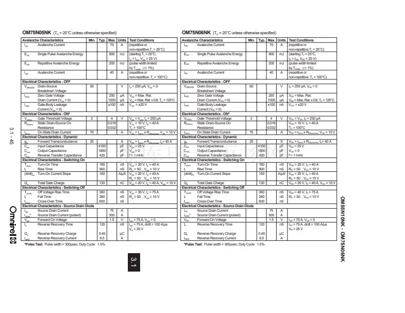 2
2
 3
3
