鈩?/div>
100% AVALANCHE TESTED
LOW CAPACITANCE AND GATE CHARGE
175
o
C MAXIMUM JUNCTION
TEMPERATURE
1
3
2
DESCRIPTION
This fully clamped Mosfet is produced by using the latest
advanced Company鈥檚 Mesh Overlay process which is
based on a novel strip layout.
The inherent benefits of the new technology coupled with
the extra clamping capabilities make this product
particularly suitable for the harshest operation conditions
such as those encountered in the automotive
environment. Any other application requiring extra
ruggedness is also recommended.
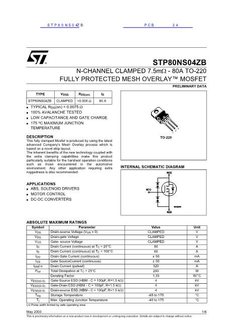
TO-220
INTERNAL SCHEMATIC DIAGRAM
APPLICATIONS
s
ABS, SOLENOID DRIVERS
s
MOTOR CONTROL
s
DC-DC CONVERTERS
ABSOLUTE MAXIMUM RATINGS
Symbol
V
DS
V
DG
V
GS
I
D
I
D
I
DG
I
GS
I
DM
(鈥?
P
tot
V
ESD(G-S)
V
ESD(G-D)
V
ESD(D-S)
T
stg
T
j
Parameter
Drain-source Voltage (V
GS
= 0)
Drain-gate Voltage
Gate- source Voltage
Drain Current (continuous) at T
C
= 25掳C
Drain Current (continuous) at T
C
= 100掳C
Drain Gate Current (continuous)
Gate SourceCurrent (continuous)
Drain Current (pulsed)
Total Dissipation at T
C
= 25掳C
Derating Factor
Gate-Source ESD (HBM - C = 100pF, R=1.5 k鈩?
Gate-Drain ESD (HBM - C = 100pF, R=1.5 k鈩?
Drain-source ESD (HBM - C = 100pF, R=1.5 k鈩?
Storage Temperature
Max. Operating Junction Temperature
Value
CLAMPED
CLAMPED
CLAMPED
80
60
卤 50
卤 50
320
200
1.33
4
4
4
-65 to 175
-40 to 175
Unit
V
V
V
A
A
mA
mA
A
W
W/掳C
kV
kV
kV
掳C
掳C
(鈥?
Pulse width limited by safe operating area.
May 2003
This is preliminary information on a new product now in development or undergoing evaluation. Details are subject to change without notice.
1/6


 1
1
 2
2
 3
3
 4
4
 5
5
 6
6
