V320 8-Bit Registered Bus Transceiver
April 1998
Revised October 1998
V320
8-Bit Registered Bus Transceiver
General Description
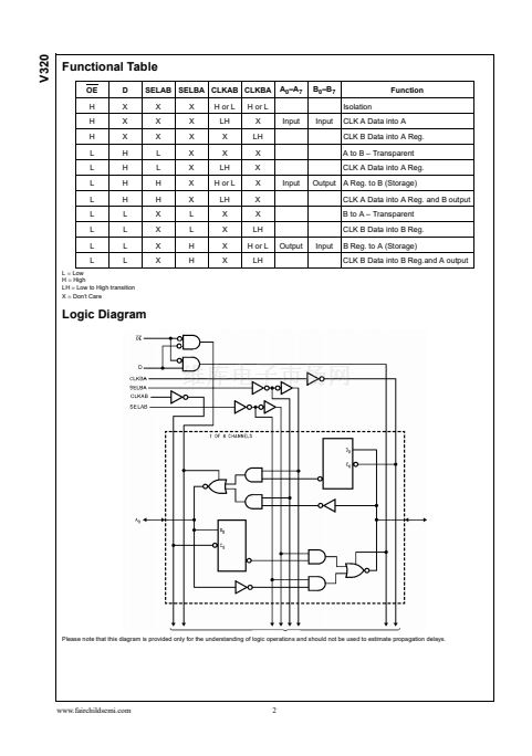
The V320 is an 8-bit universal bus transceiver designed for
high speed interfacing with the VME320 backplane. It has
output characteristics optimized for driving large capacitive
loads and features modified input levels (V
IH
/V
IL
) for
increased noise immunity and reduced input skew. The
V320 functionality consists of bus transceiver circuits with
3-STATE, D-type flip-flops, and control circuitry arranged
for multiplexed transmission of data directly from the input
bus or from the internal registers. Data on the A or B bus
will be clocked into the registers as the appropriate clock
pin goes to a high logic level. OE and direction pins are
provided to control the transceiver function. In the trans-
ceiver mode, data present at the high impedance port may
be stored in either the A or B register or in both. The select
controls can multiplex stored and real time (transparent
mode) data. The direction control determines which bus
will receive data when the enable control OE is active
LOW. In the isolation mode (OE HIGH) A data may be
stored in the B register and/or B data may be stored in the
A register.
Features
s
Independent registers for A and B buses
s
Multiplexed real-time and stored data
s
Guaranteed output skew
s
Guaranteed MOS (Multiple Output Switching) Specifica-
tions
s
Output switching specified for both 50 pF and 250 pF,
and 500 pF loads
s
Guaranteed simultaneous switching noise level (V
OLP
/
V
OLV
) and dynamic threshold performance (V
IHD
/V
ILD
)
s
Glitch free power up/down high impedance for live inser-
tion
s
BiCMOS technology for high drive and low power dissi-
pation
s
鈭?0掳C
to 85掳C commercial temperature and V
CC
specifi-
cations
s
Modified specifications across V
CC
and temperature
(V
CC
=
5.0V
卤1%,
T
=
25掳C
卤
20掳C) present more realis-
tic system conditions
s
Available in TSSOP (MTC)
Ordering Code:
Order Number
V320MTC
Package Number
MTC24
Package Description
24-Lead Thin Shrink Small Outline Package, JEDEC MO-153, 4.4mm Wide
Device also available in Tape and Reel. Specify by appending suffix letter 鈥淴鈥?to the ordering code.
Connection Diagram
Pin Descriptions
Pin Names
D
OE
CLKAB/SELAB
CLKBA/SELBA
A0鈥?
B0鈥?
Description
Direction A-to-B (High) B-to A (Low)
Output Enable (Active LOW)
A-to-B Clock/Select
B-to-A Clock/Select
A Inputs/Outputs (TTL)
B Inputs/Outputs (TTL)
漏 1998 Fairchild Semiconductor Corporation
DS500149.prf
www.fairchildsemi.com


 1
1
 2
2
 3
3
 4
4
 5
5
 6
6
 7
7
 8
8
 9
9
 10
10
