A
PPLICATION
N
OTE
A V A I L A B L E
AN61 鈥?AN75 鈥?AN77 鈥?AN79 鈥?AN82
X25F064/032/016/008
SerialFlash鈩?Memory With Block Lock
TM
Protection
FEATURES
鈥?1MHz Clock Rate
鈥?SPI Serial Interface
鈥?64K/32K/16K/8K Bits
鈥?32 Byte Small Sector Program Mode
鈥?Low Power CMOS
鈥?<1
碌
A Standby Current
鈥?<5mA Active Current
鈥?1.8V 鈥?3.6V or 5V 鈥淯nivolt鈥?Read and
Program Power Supply Versions
鈥?Block Lock Protection
鈥?Protect 1/4, 1/2, or all of E
2
PROM Array
鈥?Built-in Inadvertent Program Protection
鈥?Power-Up/Power-Down protection circuitry
鈥?Program Enable Latch
鈥?Program Protect Pin
鈥?Self-Timed Program Cycle
鈥?5ms Program Cycle Time (Typical)
鈥?High Reliability
鈥?Endurance: 100,000 cycles per byte
鈥?Data Retention: 100 Years
鈥?ESD protection: 2000V on all pins
鈥?8-Lead PDlP Package
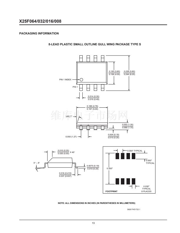
鈥?8-Lead 150 mil SOIC Packages
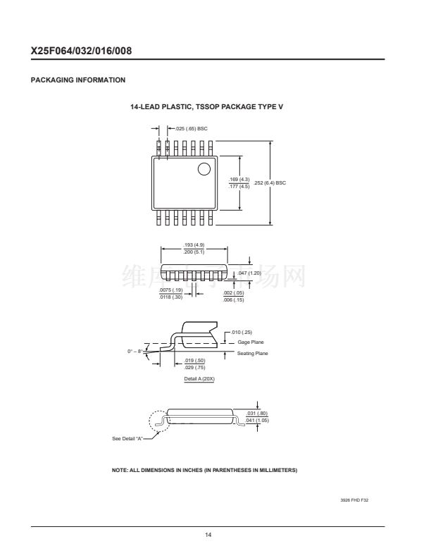
鈥?32K, 16K, 8K available in 14-Lead TSSOP,
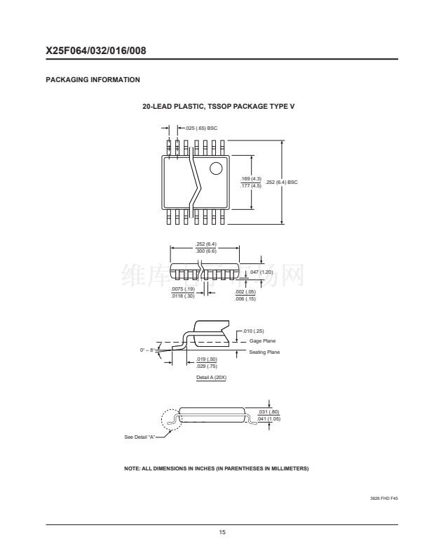
64K available in 20-Lead TSSOP
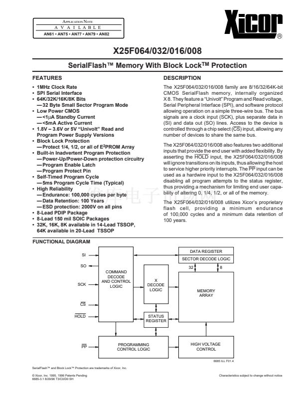
FUNCTIONAL DIAGRAM
DATA REGISTER
SI
SECTOR DECODE LOGIC
SO
COMMAND
DECODE
AND CONTROL
LOGIC
32
X
DECODE
LOGIC
8
DESCRIPTION
The X25F064/032/016/008 family are 8/16/32/64K-bit
CMOS SerialFlash memory, internally organized
X 8. They feature a 鈥淯nivolt鈥?Program and Read voltage,
Serial Peripheral Interface (SPI), and software protocol
allowing operation on a simple three-wire bus. The bus
signals are a clock input (SCK), plus separate data in
(SI) and data out (SO) lines. Access to the device is
controlled through a chip select (CS) input, allowing any
number of devices to share the same bus.
The X25F064/032/016/008 also features two additional
inputs that provide the end user with added flexibility. By
asserting the
HOLD
input, the X25F064/032/016/008
will ignore transitions on its inputs, thus allowing the host
to service higher priority interrupts. The
PP
input can be
used as a hardwire input to the X25F064/032/016/008
disabling all program attempts to the status register,
thus providing a mechanism for limiting end user capa-
bility of altering 0, 1/4, 1/2, or all of the memory.
The X25F064/032/016/008 utilizes Xicor鈥檚 proprietary
flash cell, providing a minimum endurance
of 100,000 cycles and a minimum data retention of
100 years.
SCK
MEMORY
ARRAY
CS
HOLD
STATUS
REGISTER
PP
PROGRAMMING
CONTROL LOGIC
HIGH VOLTAGE
CONTROL
6685 ILL F01.4
SerialFlash鈩?and Block Lock鈩?Protection are trademarks of Xicor, Inc.
漏 Xicor, Inc. 1995, 1996 Patents Pending
6685-3.1 8/29/96 T3/C0/D0 SH
Characteristics subject to change without notice











 1
1
 2
2
 3
3
 4
4
 5
5
 6
6
 7
7
 8
8
 9
9
 10
10
 11
11
 12
12
 13
13
 14
14
 15
15
 16
16
