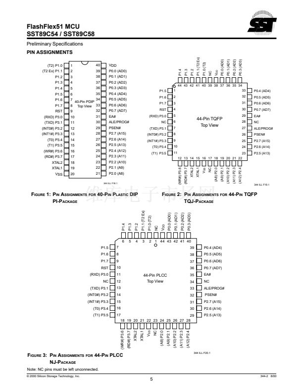
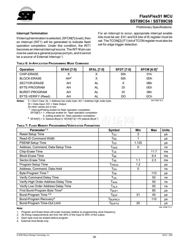
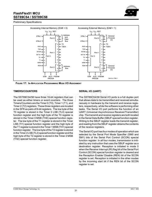
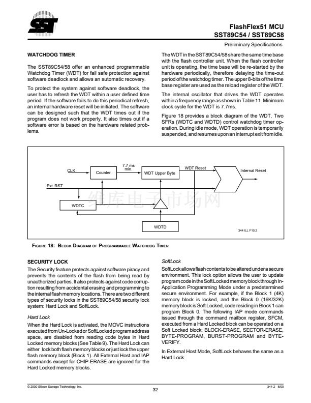
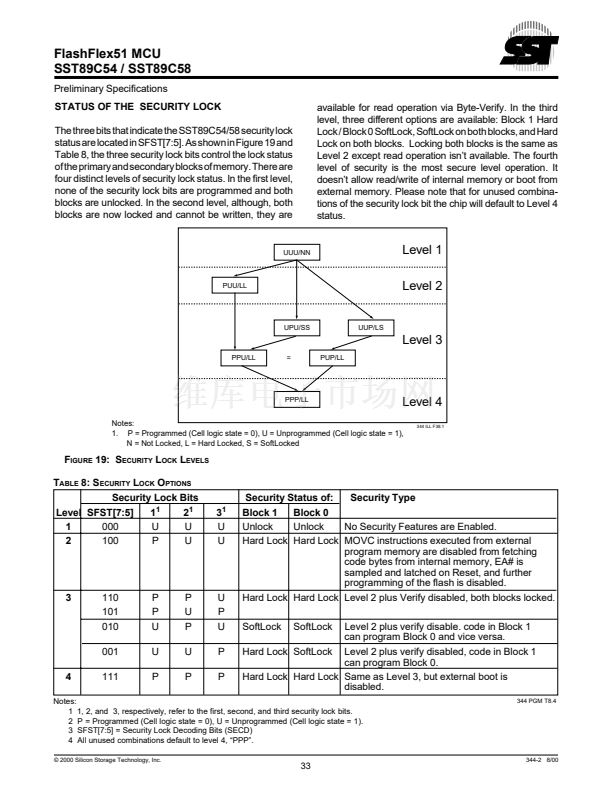
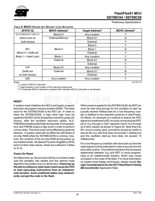
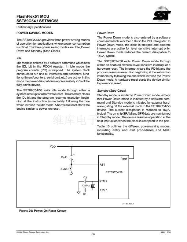
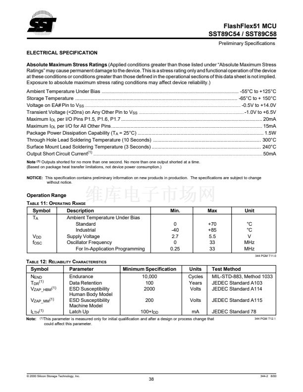
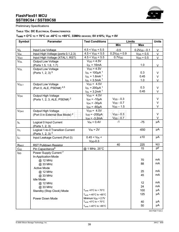
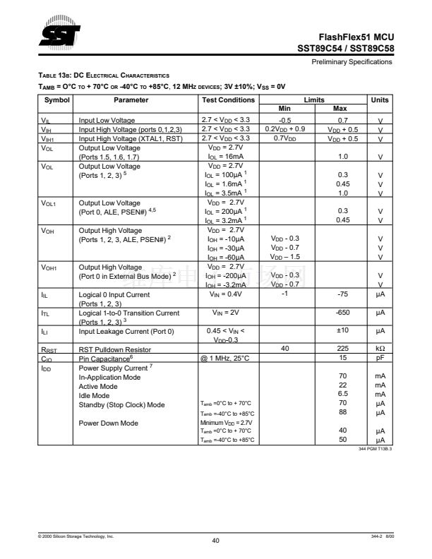
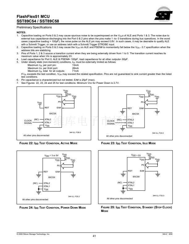
FlashFlex51 MCU
SST89C54 / SST89C58
Preliminary Specifications
EA# = 1 & SFCF[7] = 1
FFFFh
F000h
EFFFh
4 KByte
INTERNAL
(Block 1)
EA# = 1 & SFCF[7] = 0
FFFFh
FFFFh
EA# = 0
32 KByte
EXTERNAL
28 KByte
EXTERNAL
64 KByte
EXTERNAL
8000h
7FFFh
8000h
7FFFh
32 KByte
INTERNAL
(Block 0)
32 KByte
INTERNAL
(Block 0)
0000h
0000h
0000h
344 ILL F11.1
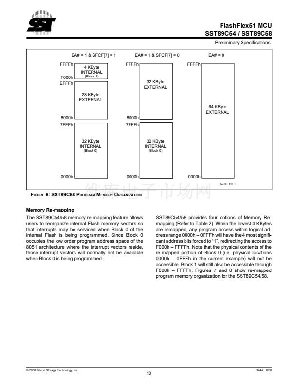
F
IGURE
6: SST89C58 P
ROGRAM
M
EMORY
O
RGANIZATION
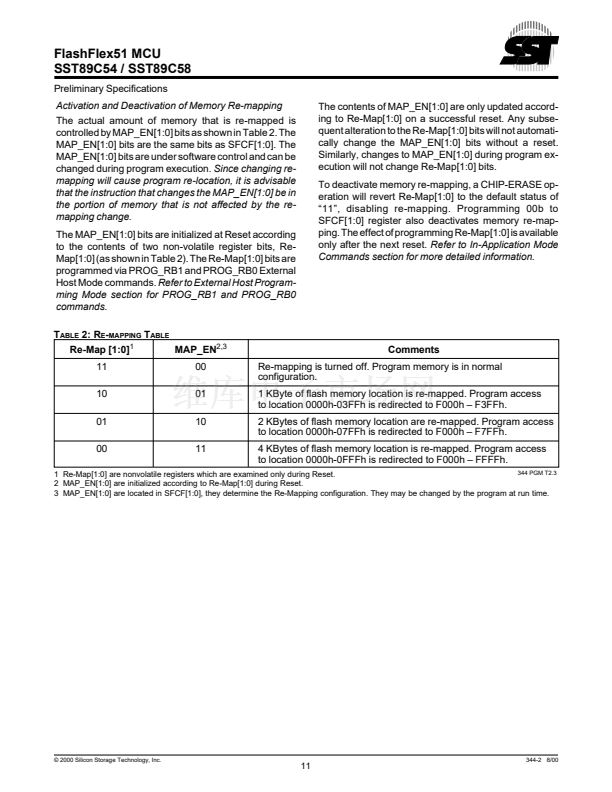
Memory Re-mapping
The SST89C54/58 memory re-mapping feature allows
users to reorganize internal Flash memory sectors so
that interrupts may be serviced when Block 0 of the
internal Flash is being programmed. Since Block 0
occupies the low order program address space of the
8051 architecture where the interrupt vectors reside,
those interrupt vectors will normally not be available
when Block 0 is being programmed.
SST89C54/58 provides four options of Memory Re-
mapping (Refer to Table 2). When the lowest 4 KBytes
are remapped, any program access within logical ad-
dress range 0000h 鈥?0FFFh will have the 4 most signifi-
cant address bits forced to 鈥?鈥? redirecting the access to
F000h 鈥?FFFFh. Note that the physical contents of the
re-mapped portion of Block 0 (i.e. physical locations
0000h 鈥?0FFFh in the current example) will not be
accessible. Block 1 will still also be accessible through
F000h 鈥?FFFFh. Figures 7 and 8 show re-mapped
program memory organization for the SST89C54/58.
漏 2000 Silicon Storage Technology, Inc.
10
344-2 8/00


 1
1
 2
2
 3
3
 4
4
 5
5
 6
6
 7
7
 8
8
 9
9
 10
10
 11
11
 12
12
 13
13
 14
14
 15
15
 16
16
 17
17
 18
18
 19
19
 20
20
 21
21
 22
22
 23
23
 24
24
 25
25
 26
26
 27
27
 28
28
 29
29
 30
30
 31
31
 32
32
 33
33
 34
34
 35
35
 36
36
 37
37
 38
38
 39
39
 40
40
 41
41
 42
42
 43
43
 44
44
 45
45
 46
46
 47
47
 48
48
 49
49
 50
50
