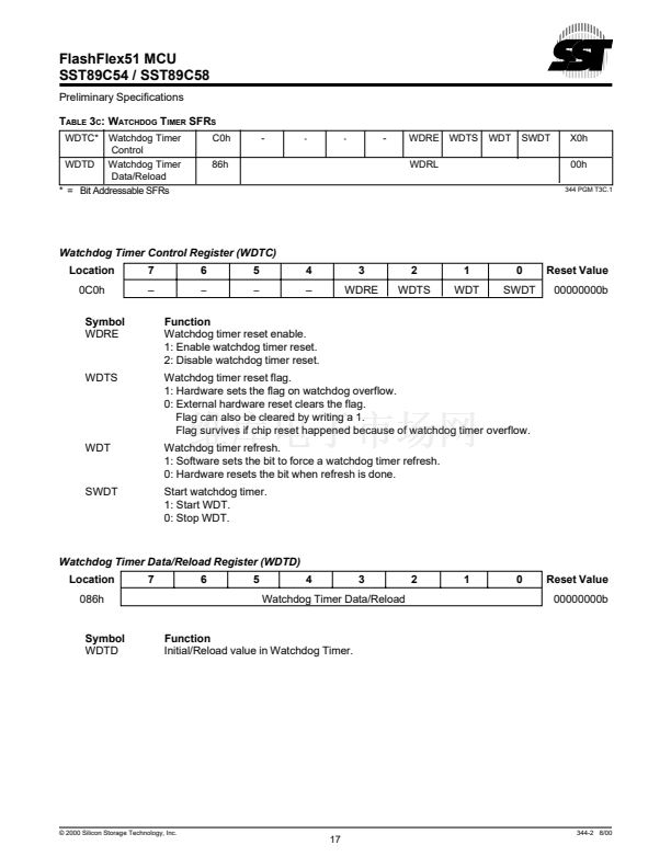
FlashFlex51 MCU
SST89C54 / SST89C58
Preliminary Specifications
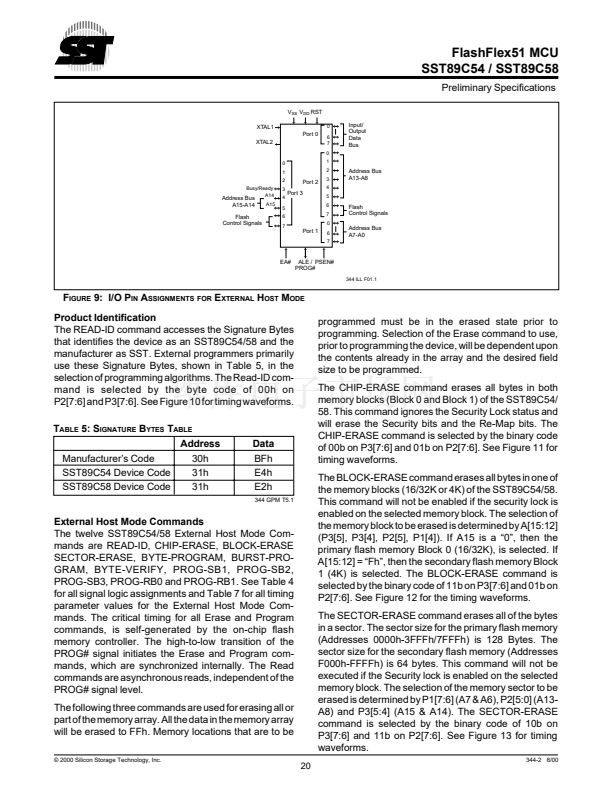
When the chip is in the External Host Mode, Port 0 pins
are assigned to be the parallel data input and output pins.
Port 1 pins are assigned to be the non-multiplexed low
order address bus signals for the internal flash memory
(A7-A0). The first six bits of Port 2 pins (P2[5:0]) are
assigned to be the non-multiplexed upper order address
bus signals for the internal flash memory (A13-A8) along
with two of the Port 3 pins (P3[5] as A15 and P3[4] as
A14). Two upper order Port 2 pins (P2[7] and P2[6]) and
two upper order Port 3 pins (P3[7] and P3[6]) along with
RST, PSEN#, PROG#/ALE, EA# pins are assigned as
the control signal pins. The Port 3 pin (P3[3]) is assigned
to be the ready/busy status signal, which can be used for
handshaking with the external host during a flash
memory programming operation. The flash memory
programming operation (Erase, Program, Verify, etc.) is
internally self-timed.
The insertion of an 鈥渁rming鈥?command prior to entering
the External Host Mode by utilizing the 鈥淩EAD-ID鈥?op-
eration provides additional protection for inadvertent
writes to the internal flash memory caused by a noisy or
unstable system environment during power-up or brown-
out conditions.
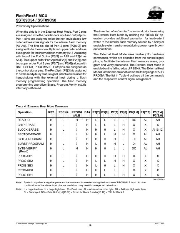
The External Host Mode uses twelve (12) hardware
commands, which are decoded from the control signal
pins, to facilitate the internal flash memory erase, pro-
gram and verify processes. The External Host Mode is
enabled on the falling edge of PSEN#. The External Host
Mode Commands are enabled on the falling edge of ALE/
PROG#. The list in Table 4 outlines all the commands
and the respective control signal assignment.
1
2
3
4
5
6
T
ABLE
4: E
XTERNAL
H
OST
M
ODE
C
OMMANDS
Operation
READ-ID
CHIP-ERASE
BLOCK-ERASE
SECTOR-ERASE
BYTE-PROGRAM
BURST-PROGRAM
BYTE-VERIFY
(Read)
PROG-SB1
PROG-SB2
PROG-SB3
PROG-RB0
PROG-RB1
RST
H
H
H
H
H
H
H
H
H
H
H
H
PSEN#
L
L
L
L
L
L
L
L
L
L
L
L
PROG# EA# P3[7] P3[6] P2[7] P2[6] P0[7:0] P1[7:0] P3[5:4]
/ALE
P2[5:0]
H
7
8
9
10
11
12
13
14
15
16
H
H
H
H
H
H
H
H
H
H
H
H
L
L
H
H
H
L
H
H
L
L
H
H
L
L
H
L
H
H
H
H
L
H
L
L
L
L
L
H
H
H
L
H
H
L
L
L
L
H
H
H
L
L
L
H
H
H
L
H
DO
X
X
X
DI
DI
DO
X
X
X
X
X
AL
X
X
AL
AL
AL
AL
X
X
X
X
X
AH
X
A[15:12]
AH
AH
AH
AH
X
X
X
X
X
344 PGM T4.4
脽
脽
脽
脽
脽
脽
脽
脽
脽
脽
H
Note:
Symbol
脽
signifies a negative pulse and the command is asserted during the low state of PROG#/ALE input. All other
combinations of the above input pins are invalid and may result in unexpected behaviors.
Note:
L = Logic low level; H = Logic high level; X = Don鈥榯 care; AL = Address low order byte; AH = Address high order byte;
DI = Data Input; DO = Data Output; A[15:12] = 0xxxb for Block 0 and A[15:12} = 鈥淔h鈥?for Block 1.
漏 2000 Silicon Storage Technology, Inc.
19
344-2 8/00


 1
1
 2
2
 3
3
 4
4
 5
5
 6
6
 7
7
 8
8
 9
9
 10
10
 11
11
 12
12
 13
13
 14
14
 15
15
 16
16
 17
17
 18
18
 19
19
 20
20
 21
21
 22
22
 23
23
 24
24
 25
25
 26
26
 27
27
 28
28
 29
29
 30
30
 31
31
 32
32
 33
33
 34
34
 35
35
 36
36
 37
37
 38
38
 39
39
 40
40
 41
41
 42
42
 43
43
 44
44
 45
45
 46
46
 47
47
 48
48
 49
49
 50
50
