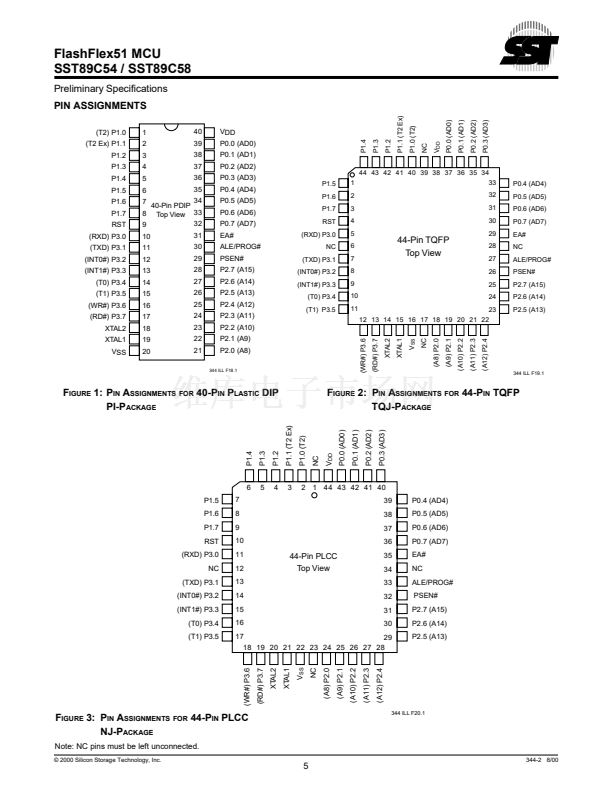
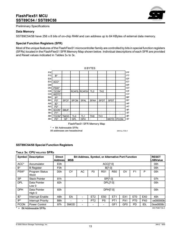
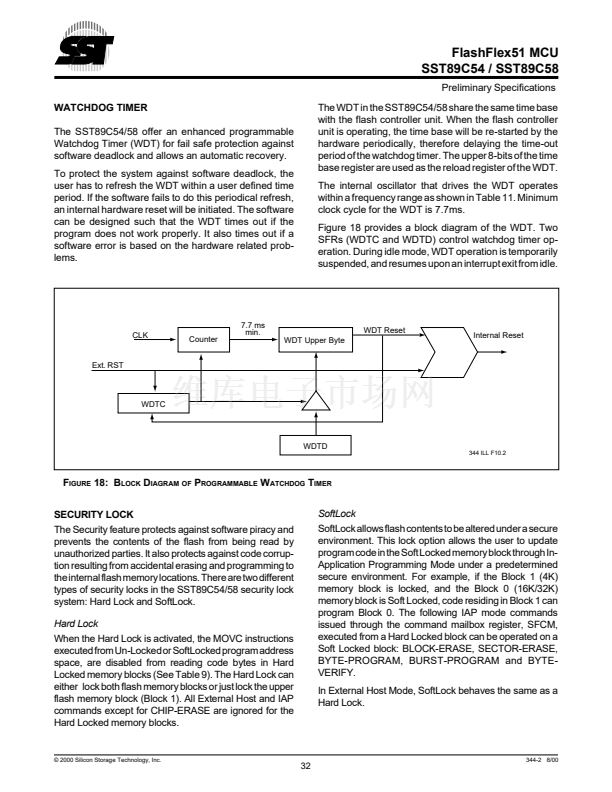
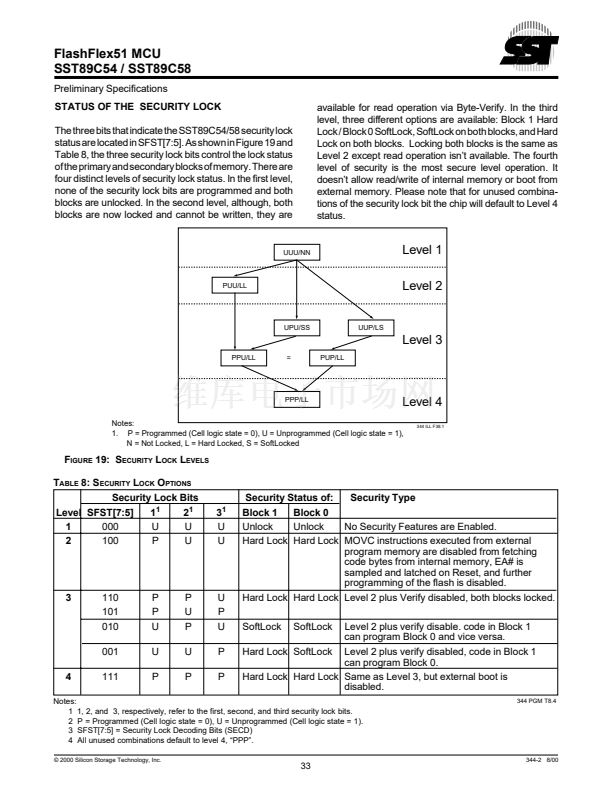
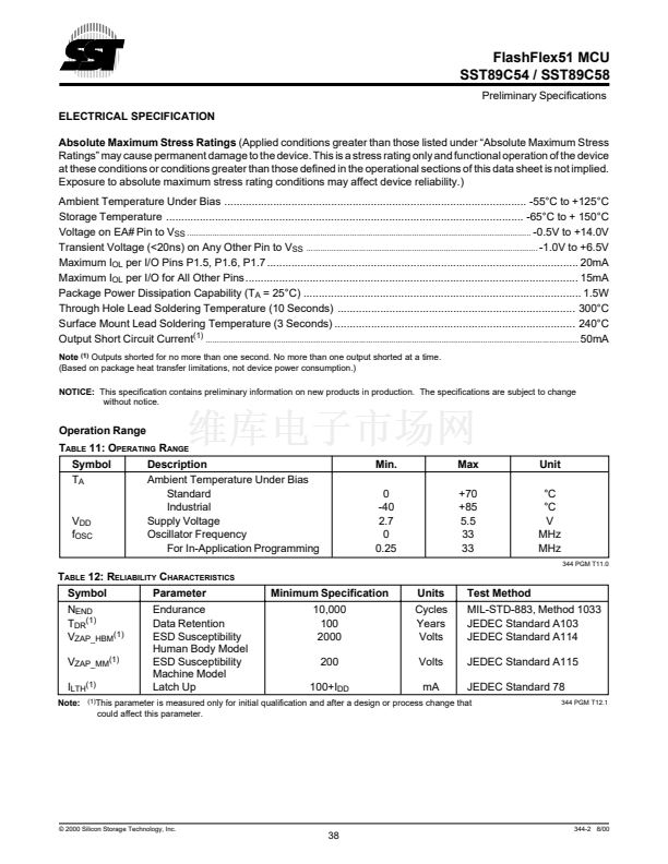
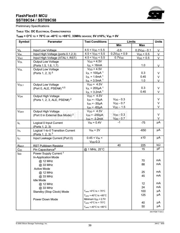
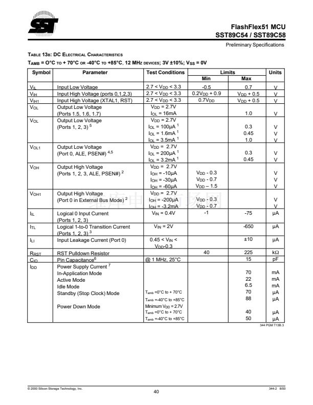
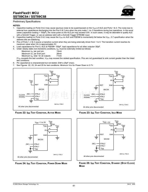
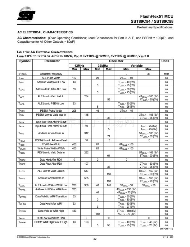
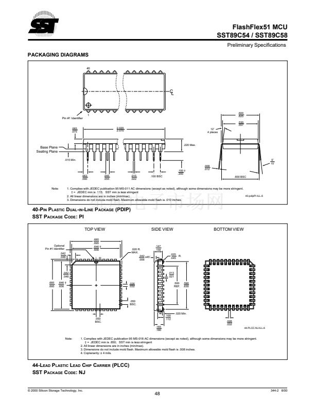
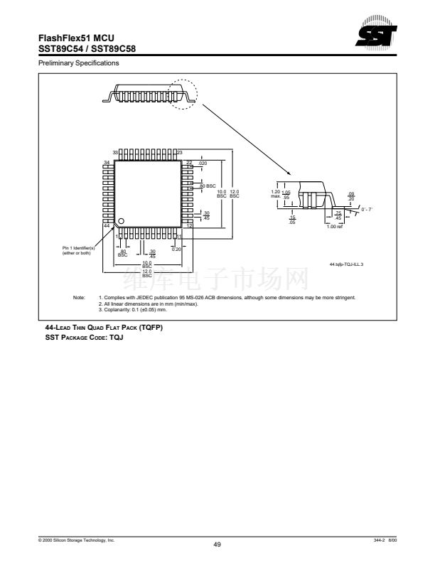
FlashFlex51 MCU
SST89C54 / SST89C58
Preliminary Specifications
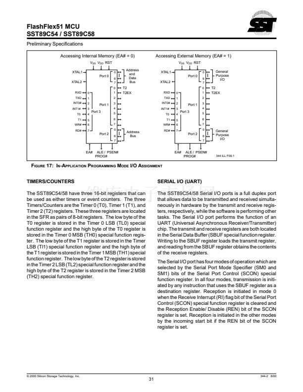
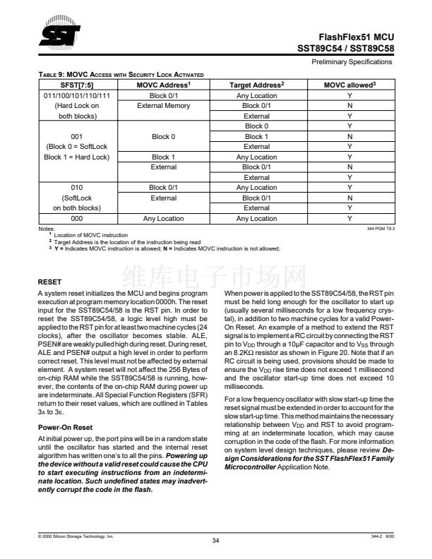
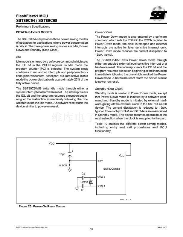
V
SS
V
DD
RST
XTAL1
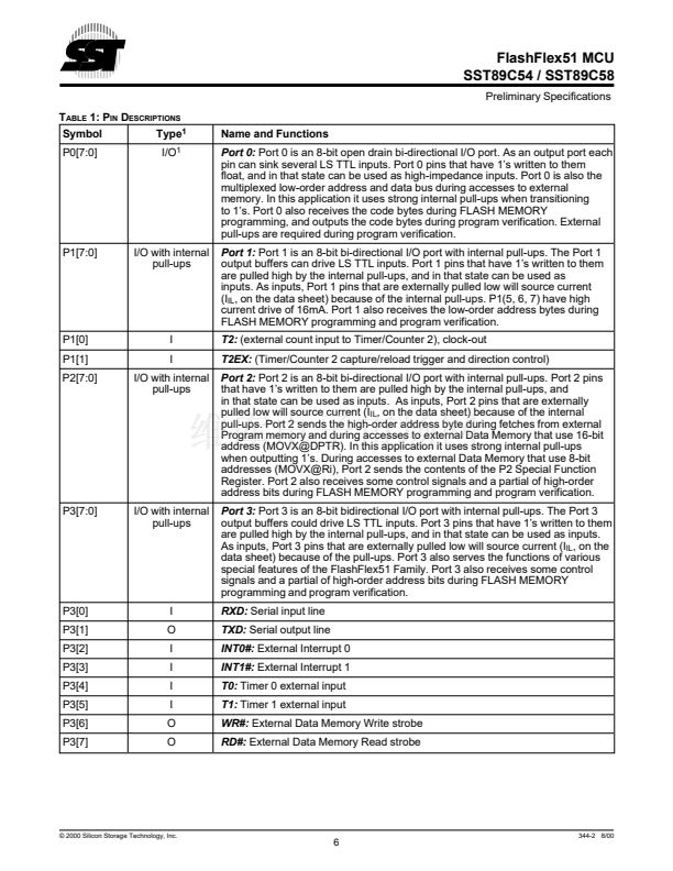
Port 0
XTAL2
0
6
7
0
0
1
2
Busy/Ready
A14
A15
3
4
5
6
7
1
2
Input/
Output
Data
Bus
Port 2
Port 3
3
4
5
6
7
0
Address Bus
A13-A8
Address Bus
A15-A14
Flash
Control Signals
Flash
Control Signals
Address Bus
A7-A0
Port 1
6
7
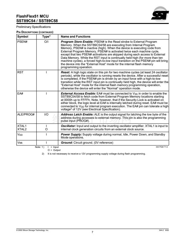
EA#
ALE / PSEN#
PROG#
344 ILL F01.1
F
IGURE
9: I/O P
IN
A
SSIGNMENTS FOR
E
XTERNAL
H
OST
M
ODE
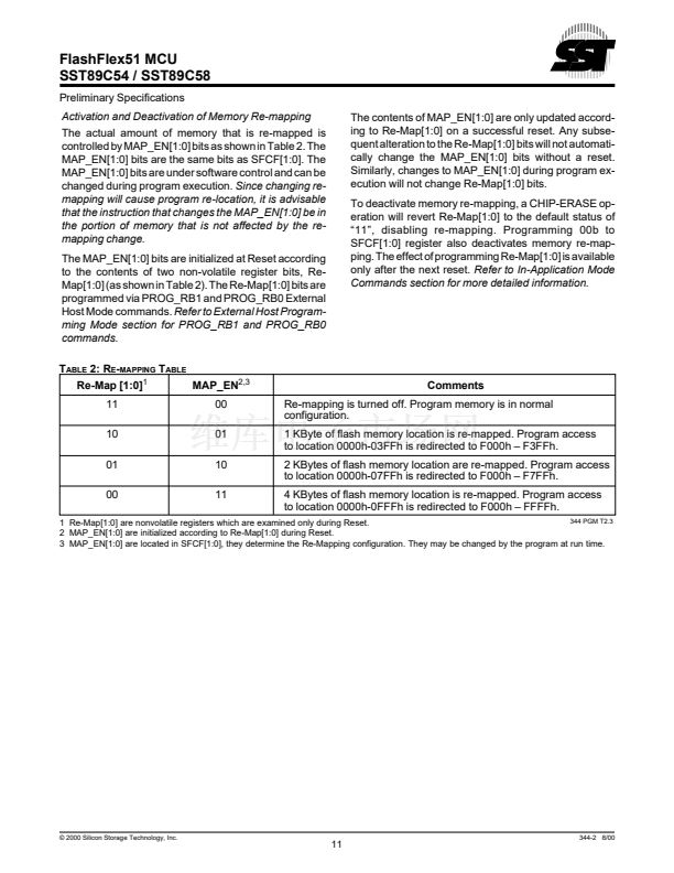
Product Identification
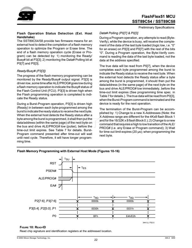
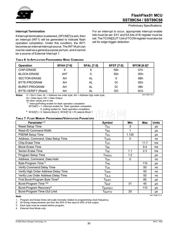
The READ-ID command accesses the Signature Bytes
that identifies the device as an SST89C54/58 and the
manufacturer as SST. External programmers primarily
use these Signature Bytes, shown in Table 5, in the
selection of programming algorithms. The Read-ID com-
mand is selected by the byte code of 00h on
P2[7:6] and P3[7:6]. See Figure 10 for timing waveforms.
T
ABLE
5: S
IGNATURE
B
YTES
T
ABLE
Address
Manufacturer鈥檚 Code
30h
SST89C54 Device Code
31h
SST89C58 Device Code
31h
programmed must be in the erased state prior to
programming. Selection of the Erase command to use,
prior to programming the device, will be dependent upon
the contents already in the array and the desired field
size to be programmed.
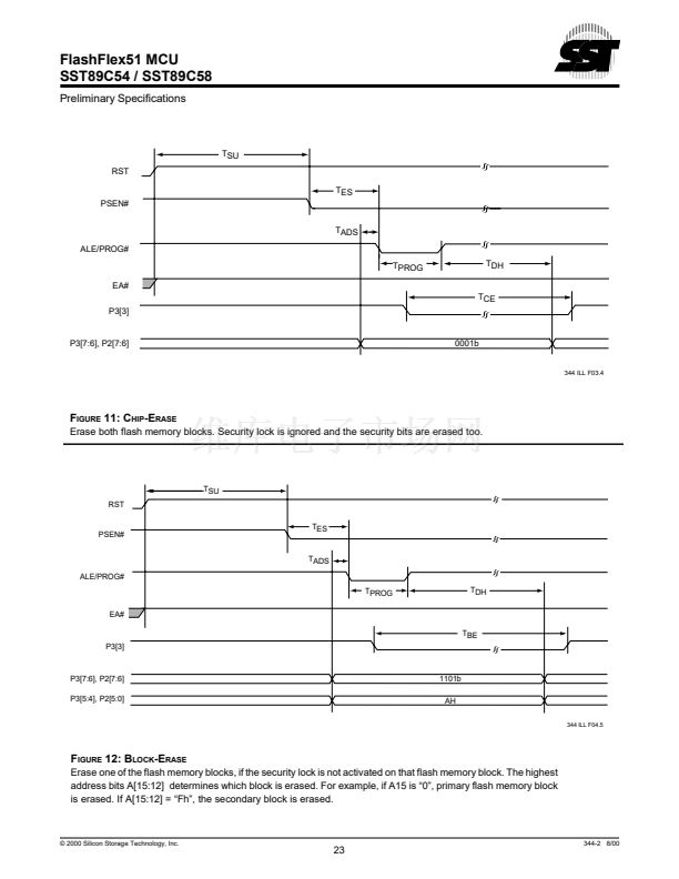
The CHIP-ERASE command erases all bytes in both
memory blocks (Block 0 and Block 1) of the SST89C54/
58. This command ignores the Security Lock status and
will erase the Security bits and the Re-Map bits. The
CHIP-ERASE command is selected by the binary code
of 00b on P3[7:6] and 01b on P2[7:6]. See Figure 11 for
timing waveforms.
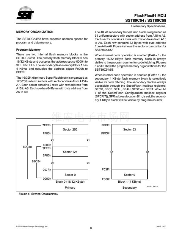
The BLOCK-ERASE command erases all bytes in one of
the memory blocks (16/32K or 4K) of the SST89C54/58.
This command will not be enabled if the security lock is
enabled on the selected memory block. The selection of
the memory block to be erased is determined by A[15:12]
(P3[5], P3[4], P2[5], P1[4]). If A15 is a 鈥?鈥? then the
primary flash memory Block 0 (16/32K), is selected. If
A[15:12] = 鈥淔h鈥? then the secondary flash memory Block
1 (4K) is selected. The BLOCK-ERASE command is
selected by the binary code of 11b on P3[7:6] and 01b on
P2[7:6]. See Figure 12 for the timing waveforms.
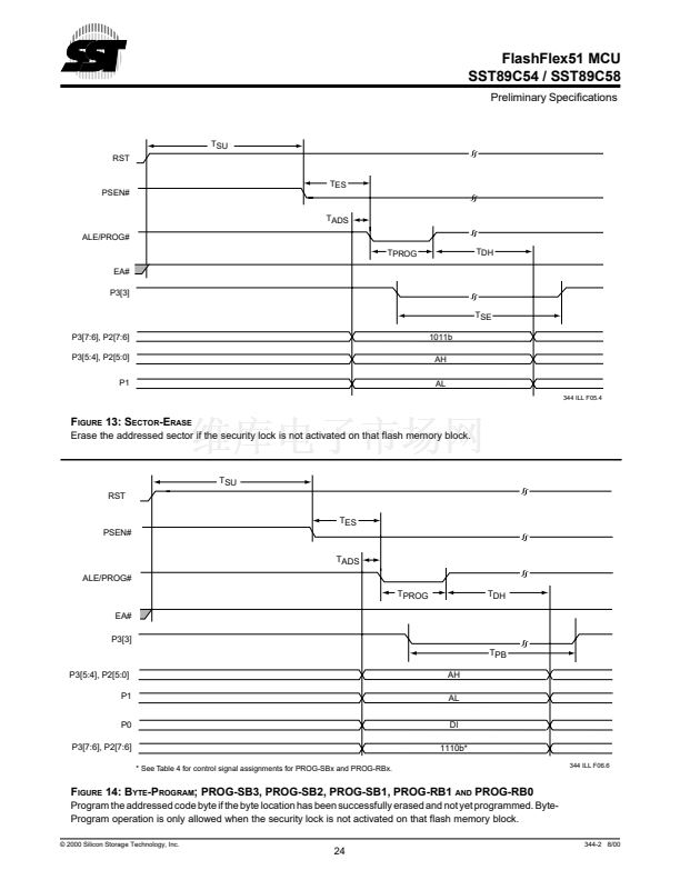
The SECTOR-ERASE command erases all of the bytes
in a sector. The sector size for the primary flash memory
(Addresses 0000h-3FFFh/7FFFh) is 128 Bytes. The
sector size for the secondary flash memory (Addresses
F000h-FFFFh) is 64 bytes. This command will not be
executed if the Security lock is enabled on the selected
memory block. The selection of the memory sector to be
erased is determined by P1[7:6] (A7 & A6), P2[5:0] (A13-
A8) and P3[5:4] (A15 & A14). The SECTOR-ERASE
command is selected by the binary code of 10b on
P3[7:6] and 11b on P2[7:6]. See Figure 13 for timing
waveforms.
20
344-2 8/00
Data
BFh
E4h
E2h
344 GPM T5.1
External Host Mode Commands
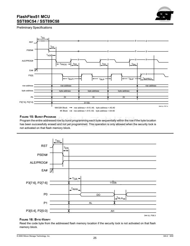
The twelve SST89C54/58 External Host Mode Com-
mands are READ-ID, CHIP-ERASE, BLOCK-ERASE
SECTOR-ERASE, BYTE-PROGRAM, BURST-PRO-
GRAM, BYTE-VERIFY, PROG-SB1, PROG-SB2,
PROG-SB3, PROG-RB0 and PROG-RB1. See Table 4
for all signal logic assignments and Table 7 for all timing
parameter values for the External Host Mode Com-
mands. The critical timing for all Erase and Program
commands, is self-generated by the on-chip flash
memory controller. The high-to-low transition of the
PROG# signal initiates the Erase and Program com-
mands, which are synchronized internally. The Read
commands are asynchronous reads, independent of the
PROG# signal level.
The following three commands are used for erasing all or
part of the memory array. All the data in the memory array
will be erased to FFh. Memory locations that are to be
漏 2000 Silicon Storage Technology, Inc.


 1
1
 2
2
 3
3
 4
4
 5
5
 6
6
 7
7
 8
8
 9
9
 10
10
 11
11
 12
12
 13
13
 14
14
 15
15
 16
16
 17
17
 18
18
 19
19
 20
20
 21
21
 22
22
 23
23
 24
24
 25
25
 26
26
 27
27
 28
28
 29
29
 30
30
 31
31
 32
32
 33
33
 34
34
 35
35
 36
36
 37
37
 38
38
 39
39
 40
40
 41
41
 42
42
 43
43
 44
44
 45
45
 46
46
 47
47
 48
48
 49
49
 50
50
