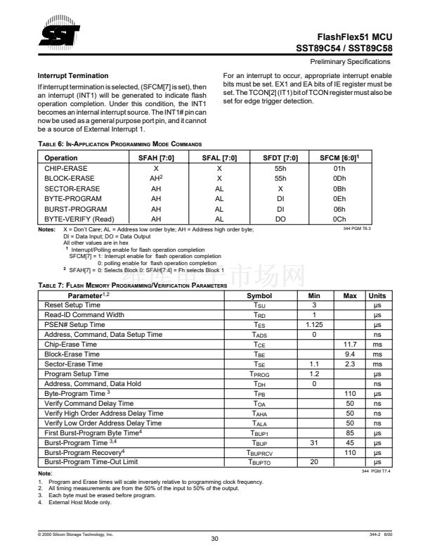
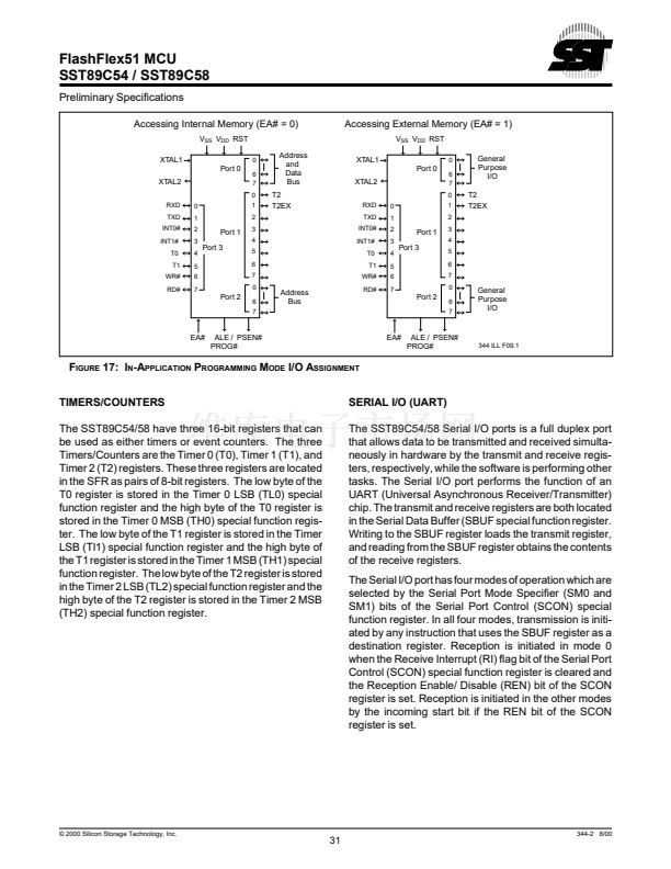
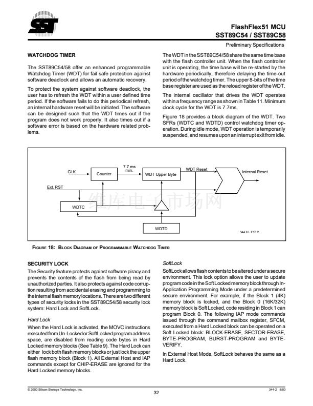
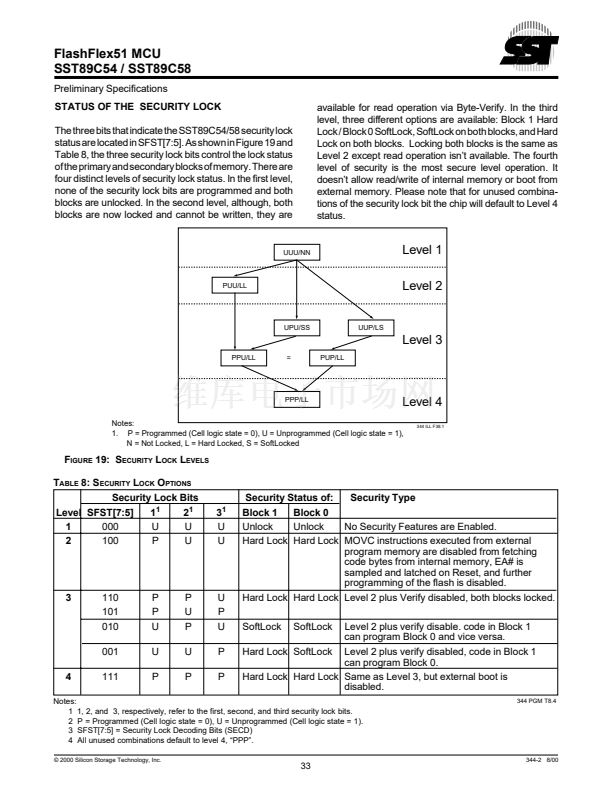
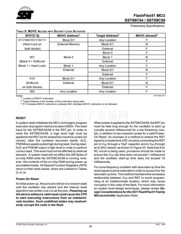
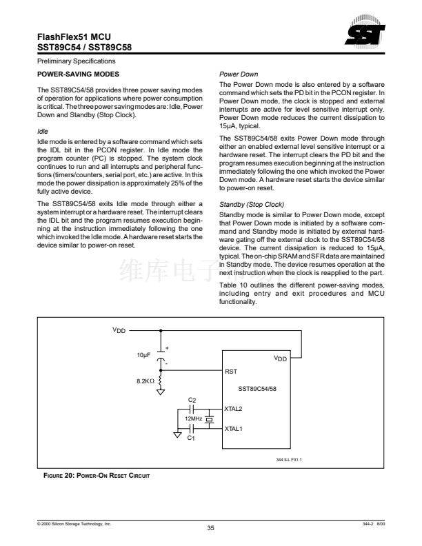
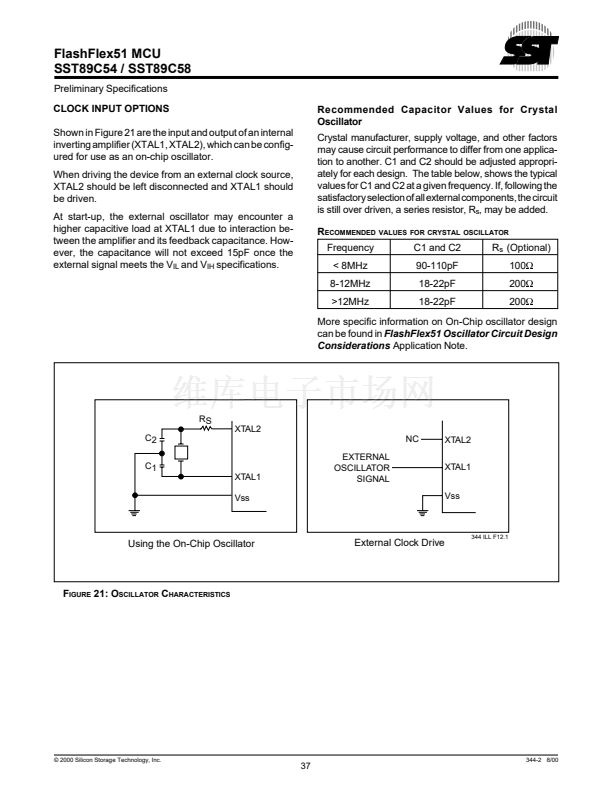
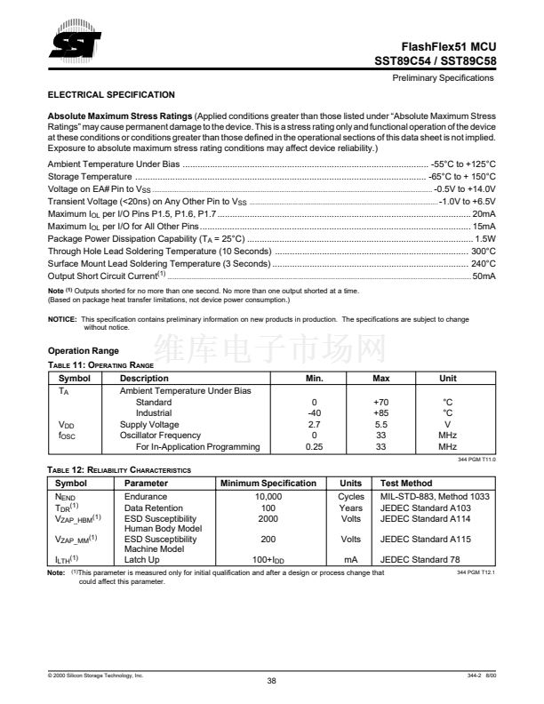
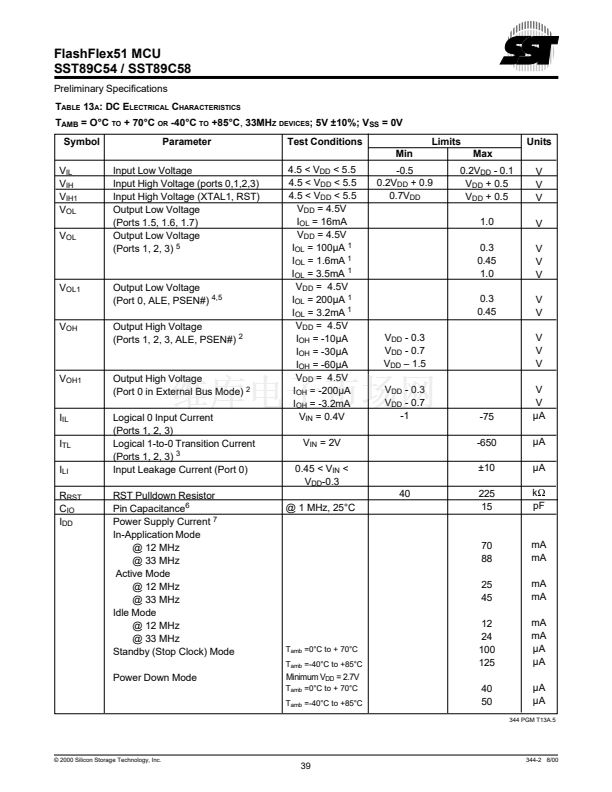
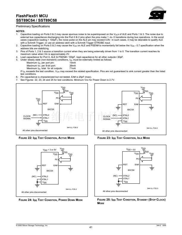
FlashFlex51 MCU
SST89C54 / SST89C58
Preliminary Specifications
T
ABLE
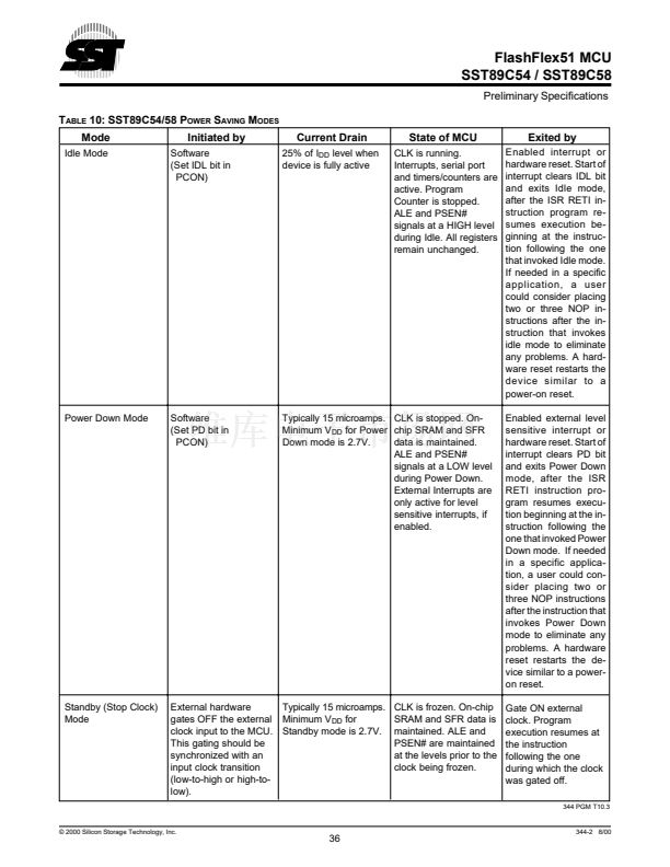
10: SST89C54/58 P
OWER
S
AVING
M
ODES
Mode
Idle Mode
Initiated by
Software
(Set IDL bit in
PCON)
Current Drain
25% of I
DD
level when
device is fully active
State of MCU
CLK is running.
Interrupts, serial port
and timers/counters are
active. Program
Counter is stopped.
ALE and PSEN#
signals at a HIGH level
during Idle. All registers
remain unchanged.
Exited by
Enabled interrupt or
hardware reset. Start of
interrupt clears IDL bit
and exits Idle mode,
after the ISR RETI in-
struction program re-
sumes execution be-
ginning at the instruc-
tion following the one
that invoked Idle mode.
If needed in a specific
application, a user
could consider placing
two or three NOP in-
structions after the in-
struction that invokes
idle mode to eliminate
any problems. A hard-
ware reset restarts the
device similar to a
power-on reset.
Enabled external level
sensitive interrupt or
hardware reset. Start of
interrupt clears PD bit
and exits Power Down
mode, after the ISR
RETI instruction pro-
gram resumes execu-
tion beginning at the in-
struction following the
one that invoked Power
Down mode. If needed
in a specific applica-
tion, a user could con-
sider placing two or
three NOP instructions
after the instruction that
invokes Power Down
mode to eliminate any
problems. A hardware
reset restarts the de-
vice similar to a power-
on reset.
Gate ON external
clock. Program
execution resumes at
the instruction
following the one
during which the clock
was gated off.
344 PGM T10.3
Power Down Mode
Software
(Set PD bit in
PCON)
Typically 15 microamps. CLK is stopped. On-
Minimum V
DD
for Power chip SRAM and SFR
Down mode is 2.7V.
data is maintained.
ALE and PSEN#
signals at a LOW level
during Power Down.
External Interrupts are
only active for level
sensitive interrupts, if
enabled.
Standby (Stop Clock)
Mode
Typically 15 microamps.
External hardware
gates OFF the external Minimum V
DD
for
clock input to the MCU. Standby mode is 2.7V.
This gating should be
synchronized with an
input clock transition
(low-to-high or high-to-
low).
CLK is frozen. On-chip
SRAM and SFR data is
maintained. ALE and
PSEN# are maintained
at the levels prior to the
clock being frozen.
漏 2000 Silicon Storage Technology, Inc.
36
344-2 8/00


 1
1
 2
2
 3
3
 4
4
 5
5
 6
6
 7
7
 8
8
 9
9
 10
10
 11
11
 12
12
 13
13
 14
14
 15
15
 16
16
 17
17
 18
18
 19
19
 20
20
 21
21
 22
22
 23
23
 24
24
 25
25
 26
26
 27
27
 28
28
 29
29
 30
30
 31
31
 32
32
 33
33
 34
34
 35
35
 36
36
 37
37
 38
38
 39
39
 40
40
 41
41
 42
42
 43
43
 44
44
 45
45
 46
46
 47
47
 48
48
 49
49
 50
50
