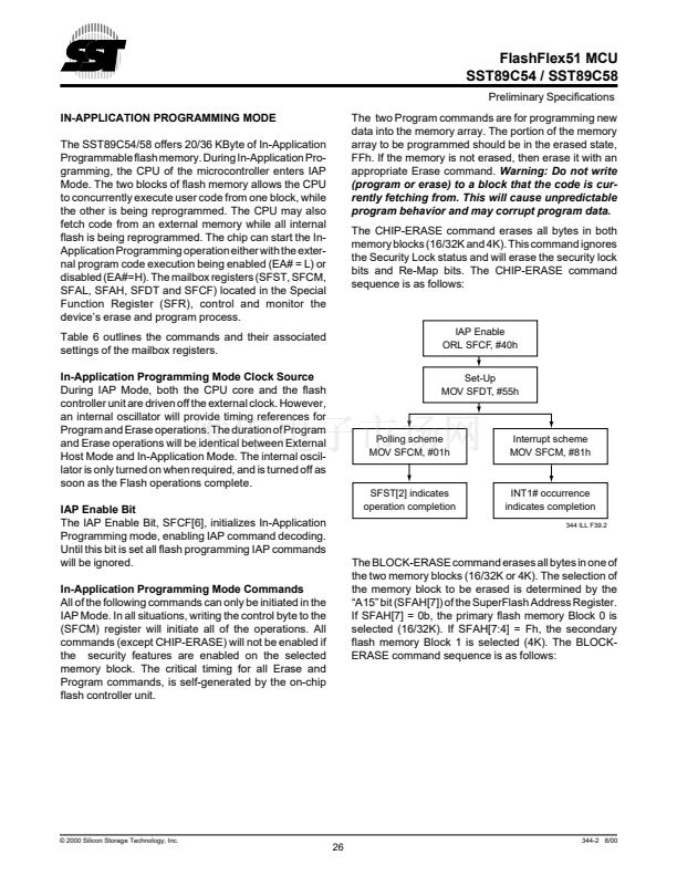
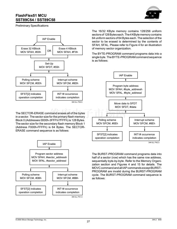
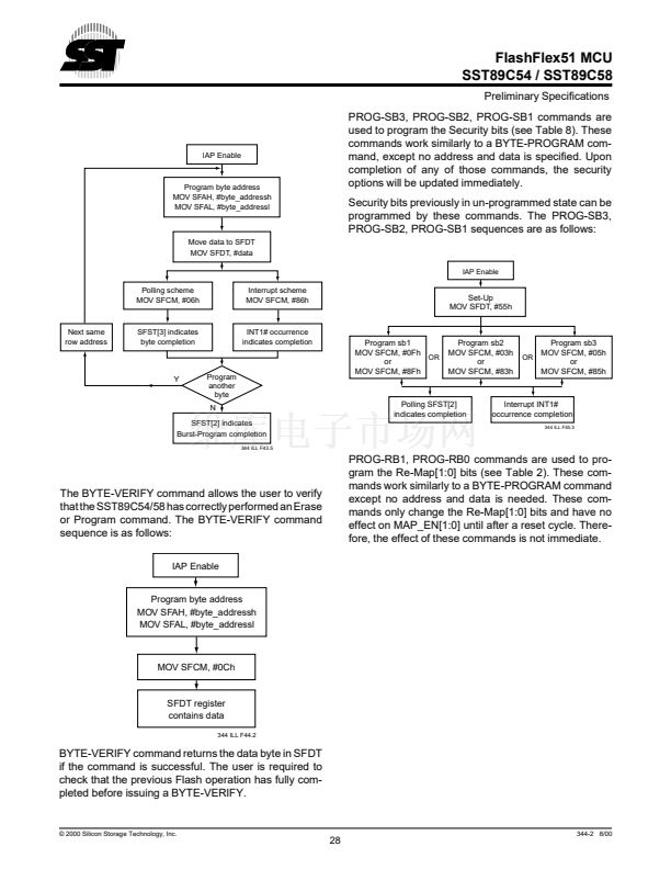
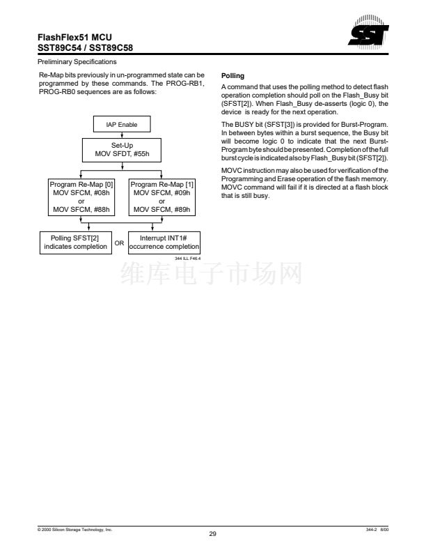
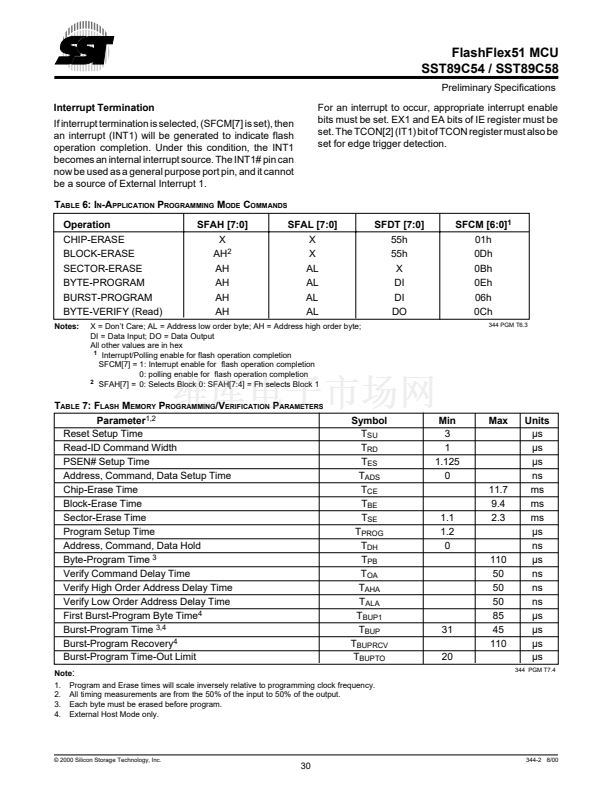
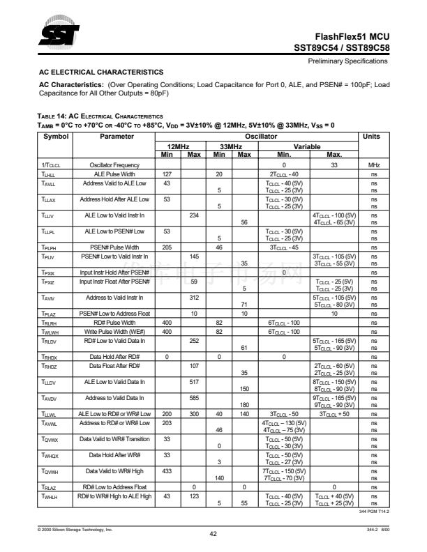
FlashFlex51 MCU
SST89C54 / SST89C58
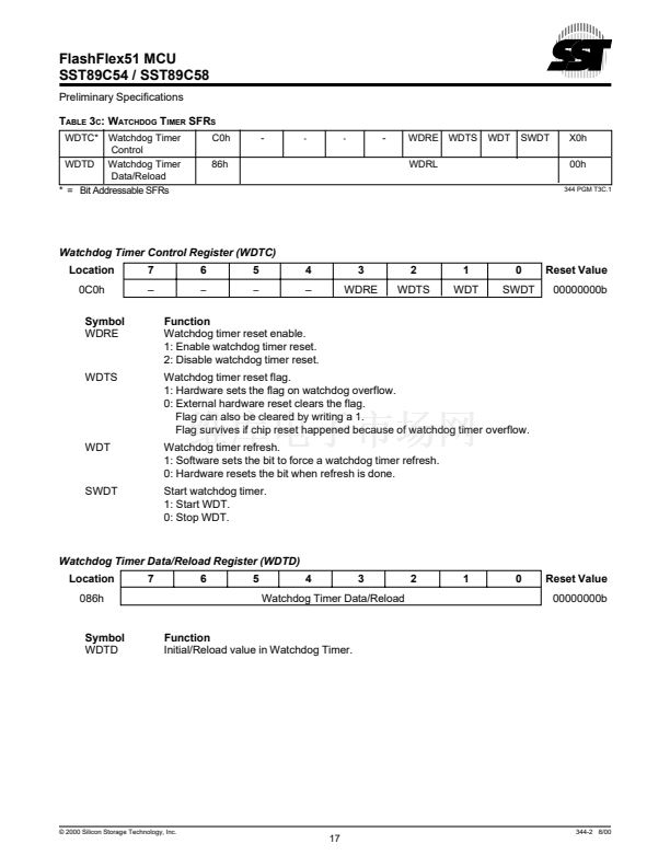
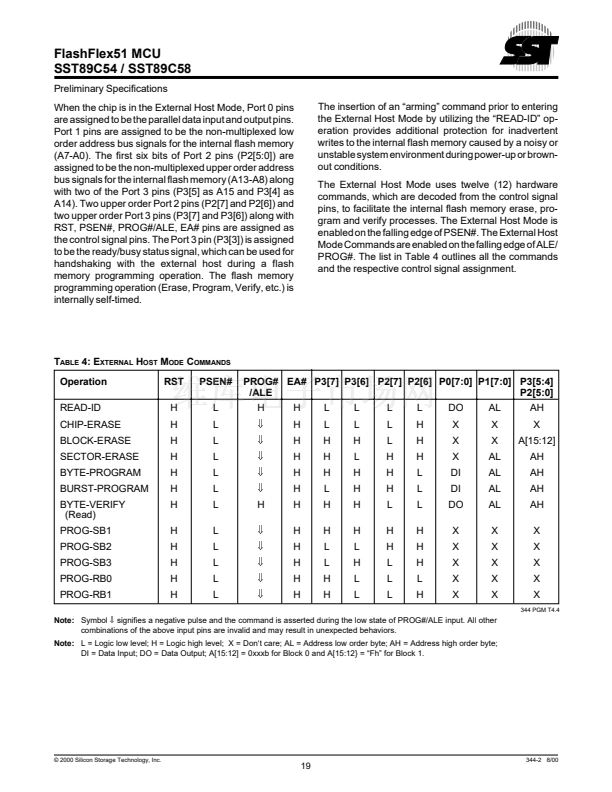
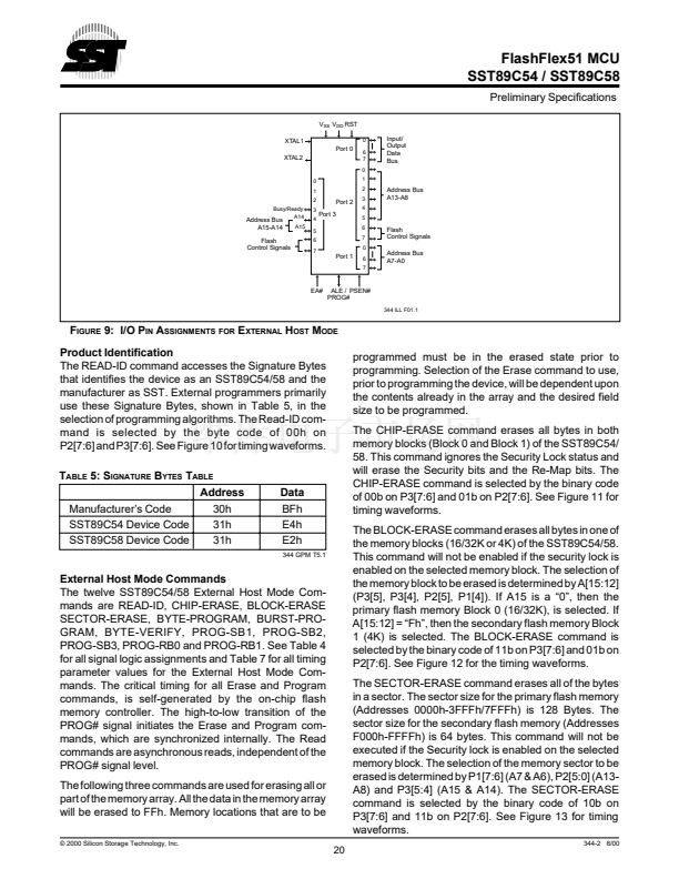
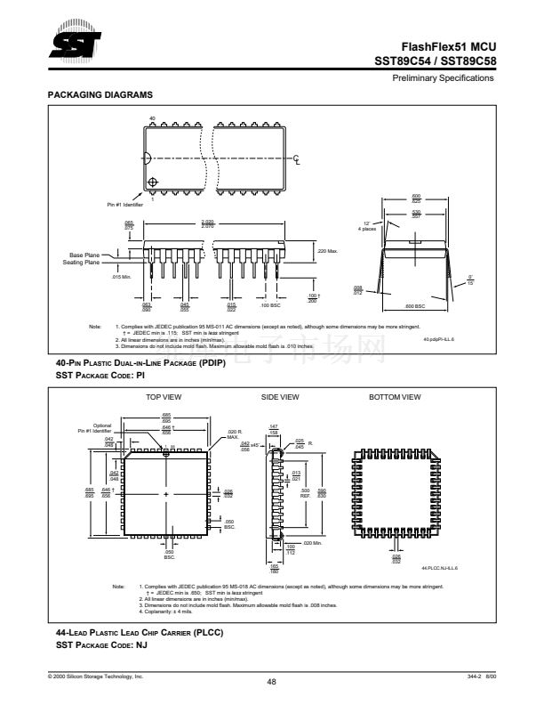
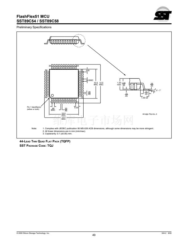
Preliminary Specifications
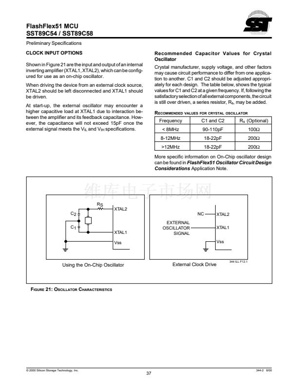
CLOCK INPUT OPTIONS
Shown in Figure 21 are the input and output of an internal
inverting amplifier (XTAL1, XTAL2), which can be config-
ured for use as an on-chip oscillator.
When driving the device from an external clock source,
XTAL2 should be left disconnected and XTAL1 should
be driven.
At start-up, the external oscillator may encounter a
higher capacitive load at XTAL1 due to interaction be-
tween the amplifier and its feedback capacitance. How-
ever, the capacitance will not exceed 15pF once the
external signal meets the V
IL
and V
IH
specifications.
Recommended Capacitor Values for Crystal
Oscillator
Crystal manufacturer, supply voltage, and other factors
may cause circuit performance to differ from one applica-
tion to another. C1 and C2 should be adjusted appropri-
ately for each design. The table below, shows the typical
values for C1 and C2 at a given frequency. If, following the
satisfactory selection of all external components, the circuit
is still over driven, a series resistor, R
s
, may be added.
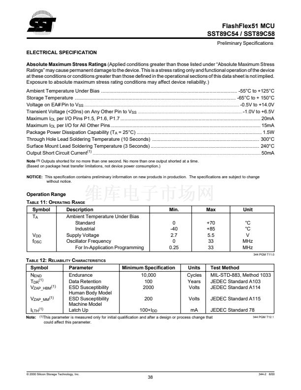
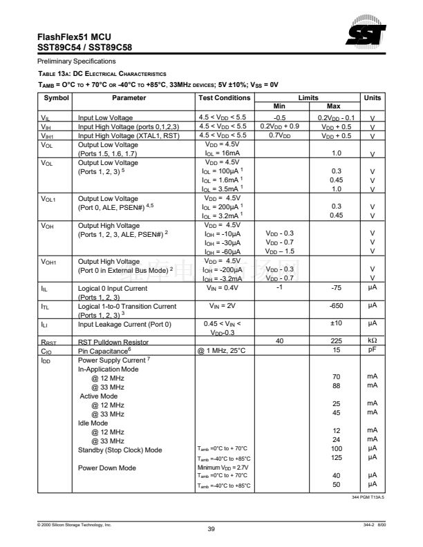
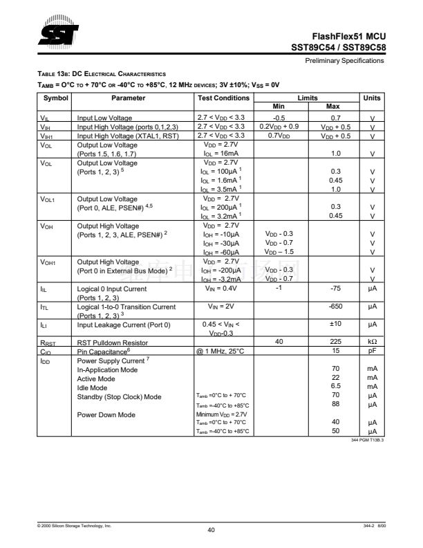
R
ECOMMENDED VALUES FOR CRYSTAL OSCILLATOR
Frequency
< 8MHz
8-12MHz
>12MHz
C1 and C2
90-110pF
18-22pF
18-22pF
R
s
(Optional)
200
W
100
W
1
2
3
4
5
6
7
8
200
W
More specific information on On-Chip oscillator design
can be found in
FlashFlex51 Oscillator Circuit Design
Considerations
Application Note.
RS
C2
C1
XTAL2
NC
EXTERNAL
OSCILLATOR
SIGNAL
XTAL2
XTAL1
Vss
9
10
11
XTAL1
Vss
Using the On-Chip Oscillator
External Clock Drive
344 ILL F12.1
12
13
F
IGURE
21: O
SCILLATOR
C
HARACTERISTICS
14
15
16
漏 2000 Silicon Storage Technology, Inc.
37
344-2 8/00


 1
1
 2
2
 3
3
 4
4
 5
5
 6
6
 7
7
 8
8
 9
9
 10
10
 11
11
 12
12
 13
13
 14
14
 15
15
 16
16
 17
17
 18
18
 19
19
 20
20
 21
21
 22
22
 23
23
 24
24
 25
25
 26
26
 27
27
 28
28
 29
29
 30
30
 31
31
 32
32
 33
33
 34
34
 35
35
 36
36
 37
37
 38
38
 39
39
 40
40
 41
41
 42
42
 43
43
 44
44
 45
45
 46
46
 47
47
 48
48
 49
49
 50
50
