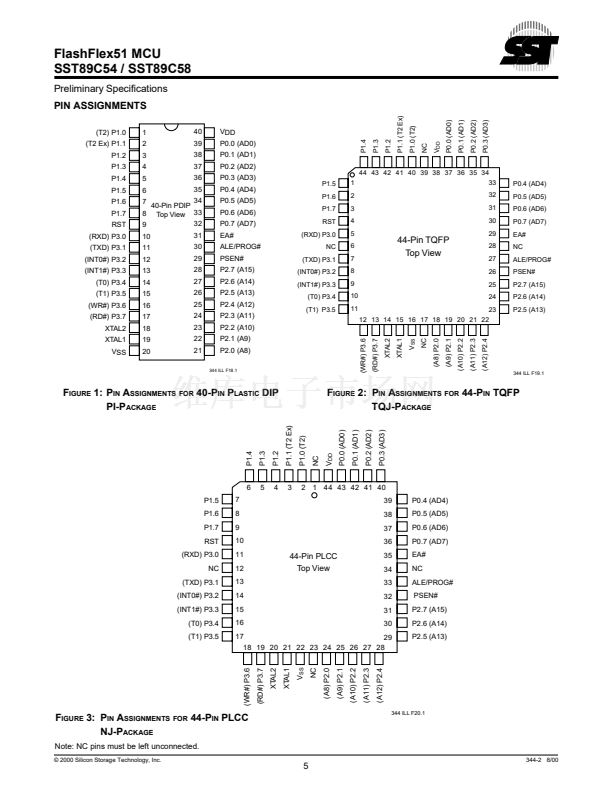
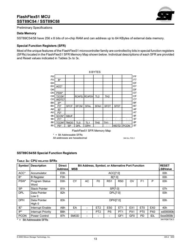
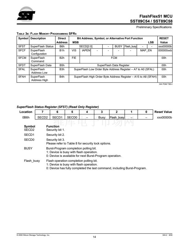
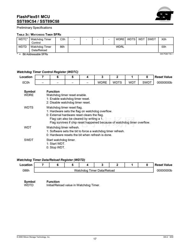
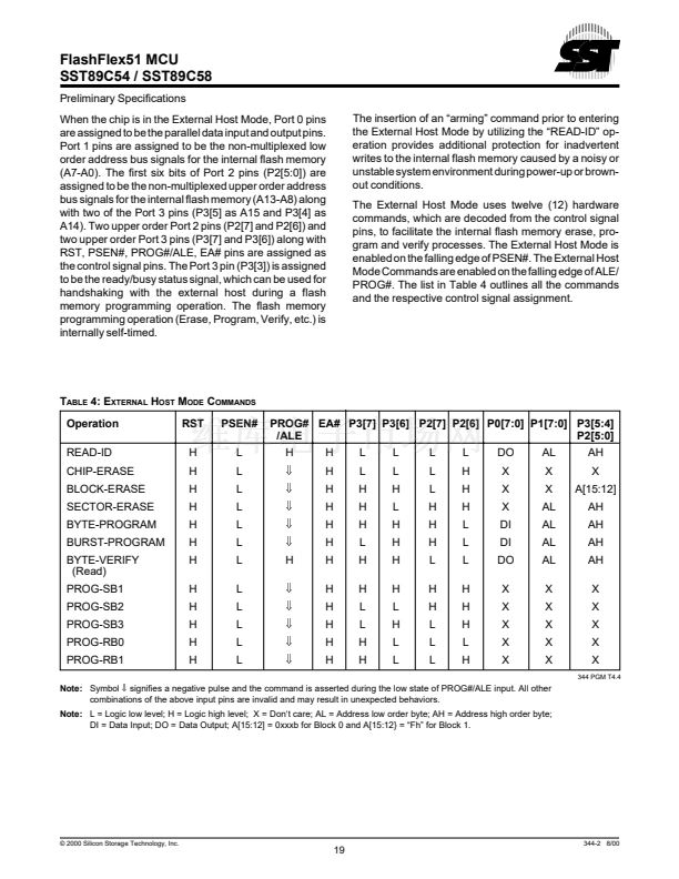
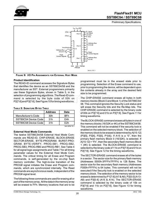
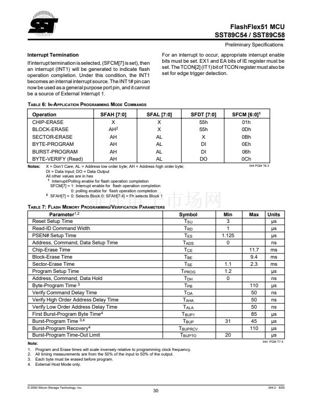
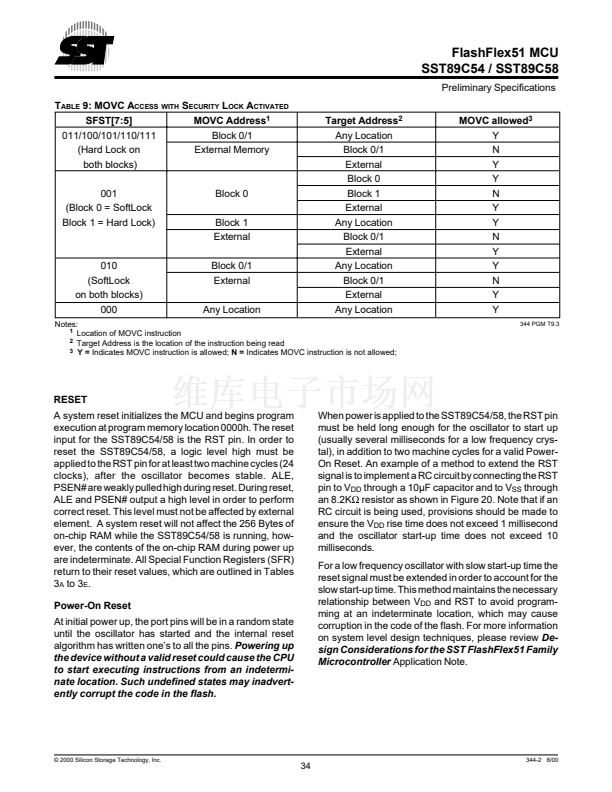
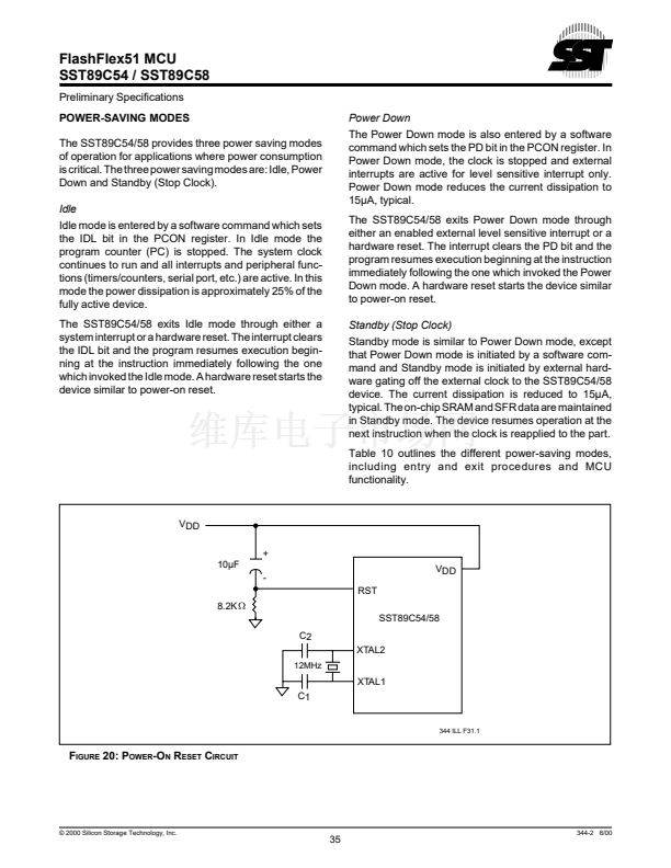
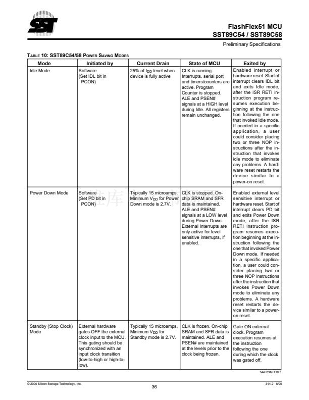
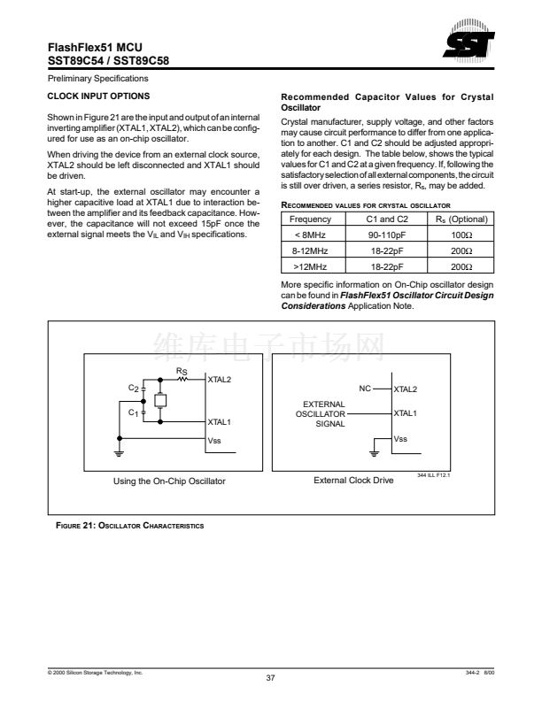
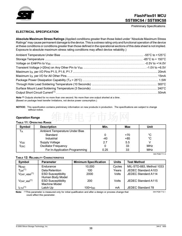
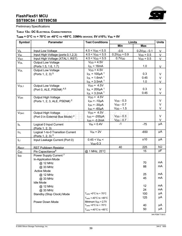
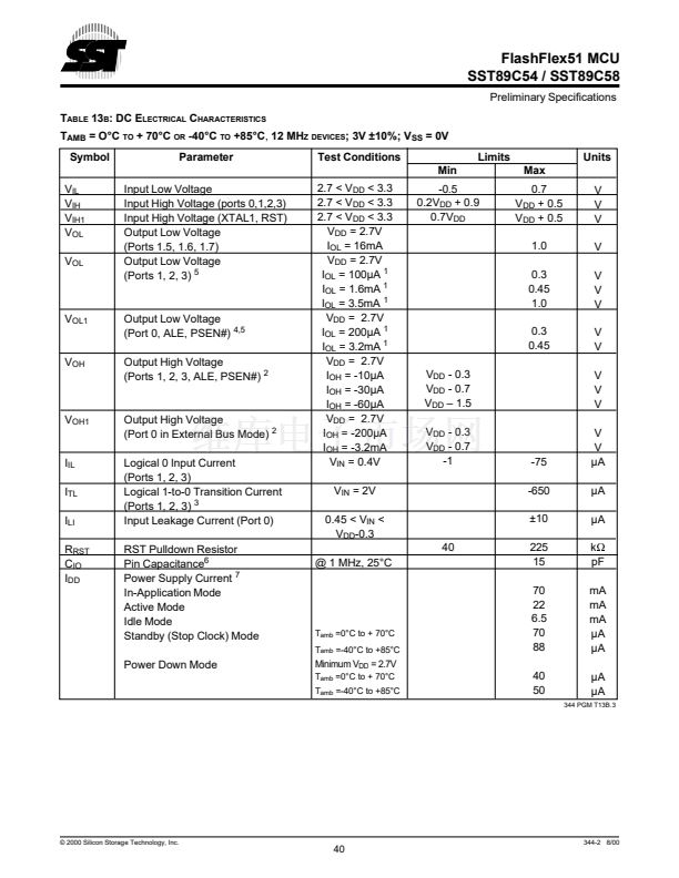
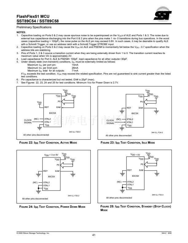
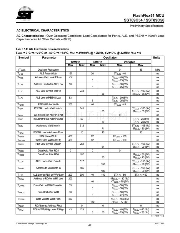
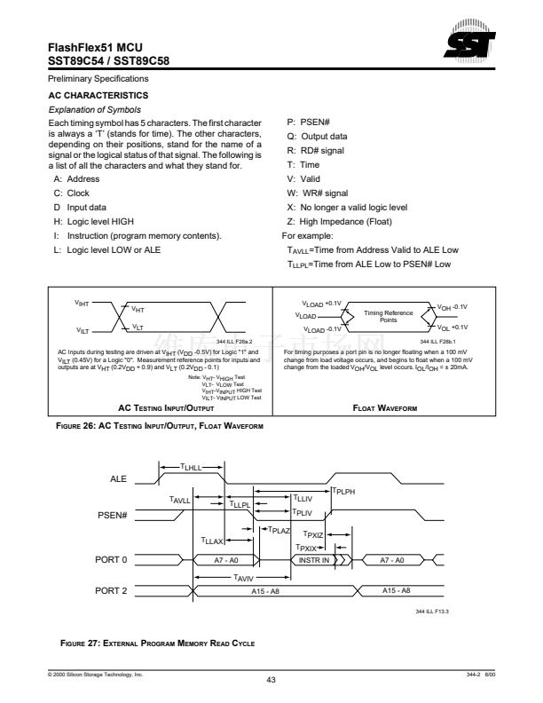
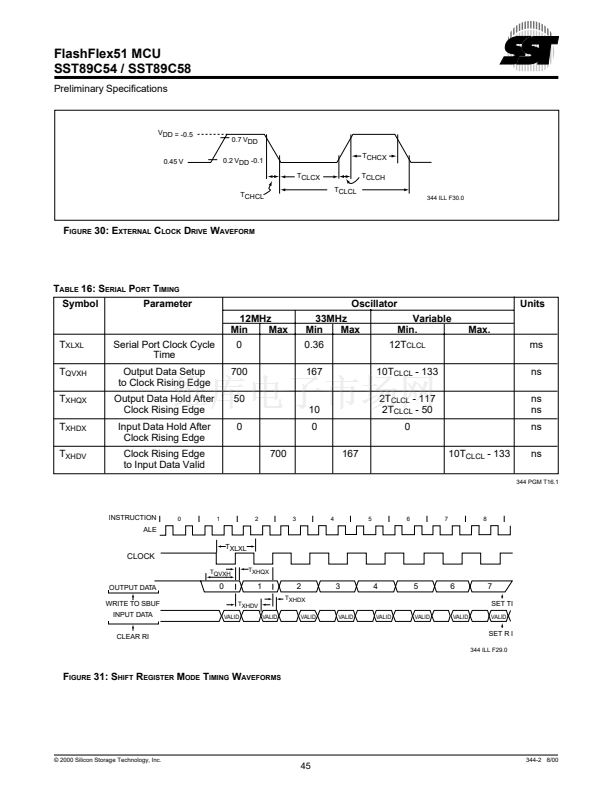
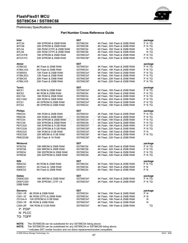
FlashFlex51 MCU
SST89C54 / SST89C58
Preliminary Specifications
T
ABLE
1: P
IN
D
ESCRIPTIONS
Symbol
Type
1
P0[7:0]
I/O
1
Name and Functions
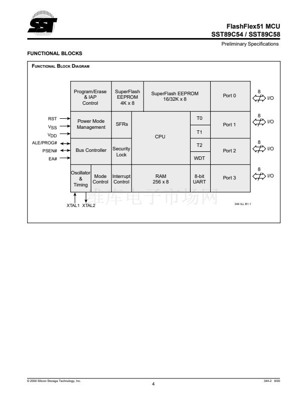
Port 0:
Port 0 is an 8-bit open drain bi-directional I/O port. As an output port each
pin can sink several LS TTL inputs. Port 0 pins that have 1鈥檚 written to them
float, and in that state can be used as high-impedance inputs. Port 0 is also the
multiplexed low-order address and data bus during accesses to external
memory. In this application it uses strong internal pull-ups when transitioning
to 1鈥檚. Port 0 also receives the code bytes during FLASH MEMORY
programming, and outputs the code bytes during program verification. External
pull-ups are required during program verification.
Port 1:
Port 1 is an 8-bit bi-directional I/O port with internal pull-ups. The Port 1
output buffers can drive LS TTL inputs. Port 1 pins that have 1鈥檚 written to them
are pulled high by the internal pull-ups, and in that state can be used as
inputs. As inputs, Port 1 pins that are externally pulled low will source current
(I
IL
, on the data sheet) because of the internal pull-ups. P1(5, 6, 7) have high
current drive of 16mA. Port 1 also receives the low-order address bytes during
FLASH MEMORY programming and program verification.
T2:
(external count input to Timer/Counter 2), clock-out
T2EX:
(Timer/Counter 2 capture/reload trigger and direction control)
Port 2:
Port 2 is an 8-bit bi-directional I/O port with internal pull-ups. Port 2 pins
that have 1鈥檚 written to them are pulled high by the internal pull-ups, and
in that state can be used as inputs. As inputs, Port 2 pins that are externally
pulled low will source current (I
IL
, on the data sheet) because of the internal
pull-ups. Port 2 sends the high-order address byte during fetches from external
Program memory and during accesses to external Data Memory that use 16-bit
address (MOVX@DPTR). In this application it uses strong internal pull-ups
when outputting 1鈥檚. During accesses to external Data Memory that use 8-bit
addresses (MOVX@Ri), Port 2 sends the contents of the P2 Special Function
Register. Port 2 also receives some control signals and a partial of high-order
address bits during FLASH MEMORY programming and program verification.
Port 3:
Port 3 is an 8-bit bidirectional I/O port with internal pull-ups. The Port 3
output buffers could drive LS TTL inputs. Port 3 pins that have 1鈥檚 written to them
are pulled high by the internal pull-ups, and in that state can be used as inputs.
As inputs, Port 3 pins that are externally pulled low will source current (I
IL
, on the
data sheet) because of the pull-ups. Port 3 also serves the functions of various
special features of the FlashFlex51 Family. Port 3 also receives some control
signals and a partial of high-order address bits during FLASH MEMORY
programming and program verification.
RXD:
Serial input line
TXD:
Serial output line
INT0#:
External Interrupt 0
INT1#:
External Interrupt 1
T0:
Timer 0 external input
T1:
Timer 1 external input
WR#:
External Data Memory Write strobe
RD#:
External Data Memory Read strobe
P1[7:0]
I/O with internal
pull-ups
P1[0]
P1[1]
P2[7:0]
I
I
I/O with internal
pull-ups
P3[7:0]
I/O with internal
pull-ups
P3[0]
P3[1]
P3[2]
P3[3]
P3[4]
P3[5]
P3[6]
P3[7]
I
O
I
I
I
I
O
O
漏 2000 Silicon Storage Technology, Inc.
6
344-2 8/00


 1
1
 2
2
 3
3
 4
4
 5
5
 6
6
 7
7
 8
8
 9
9
 10
10
 11
11
 12
12
 13
13
 14
14
 15
15
 16
16
 17
17
 18
18
 19
19
 20
20
 21
21
 22
22
 23
23
 24
24
 25
25
 26
26
 27
27
 28
28
 29
29
 30
30
 31
31
 32
32
 33
33
 34
34
 35
35
 36
36
 37
37
 38
38
 39
39
 40
40
 41
41
 42
42
 43
43
 44
44
 45
45
 46
46
 47
47
 48
48
 49
49
 50
50
