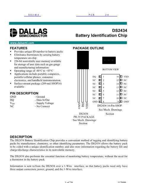
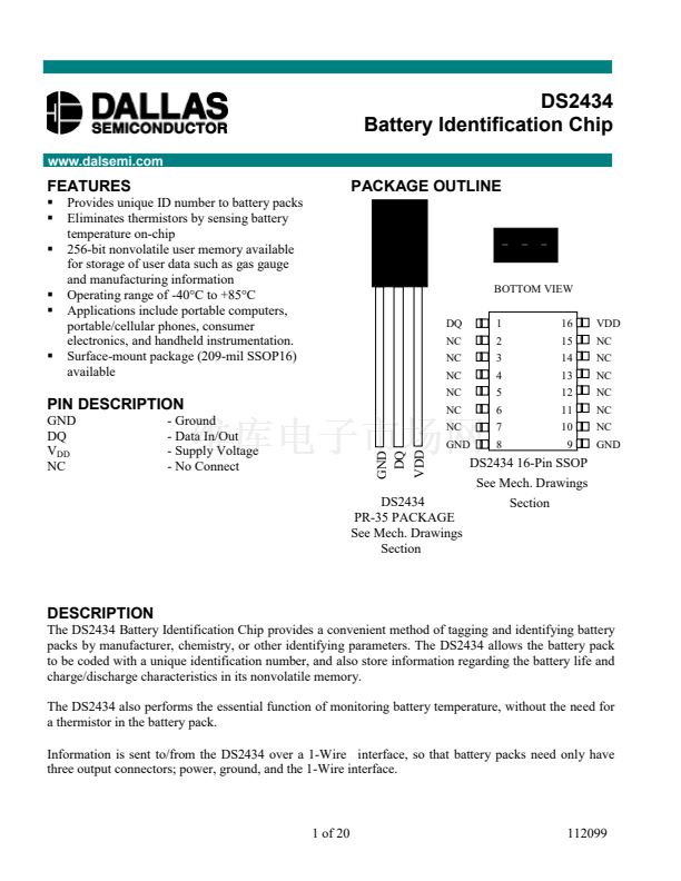
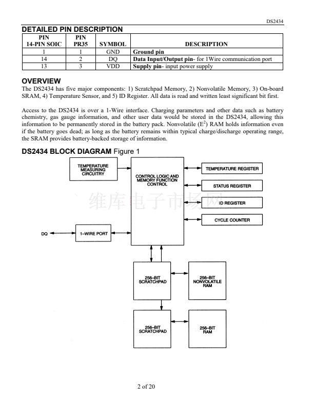
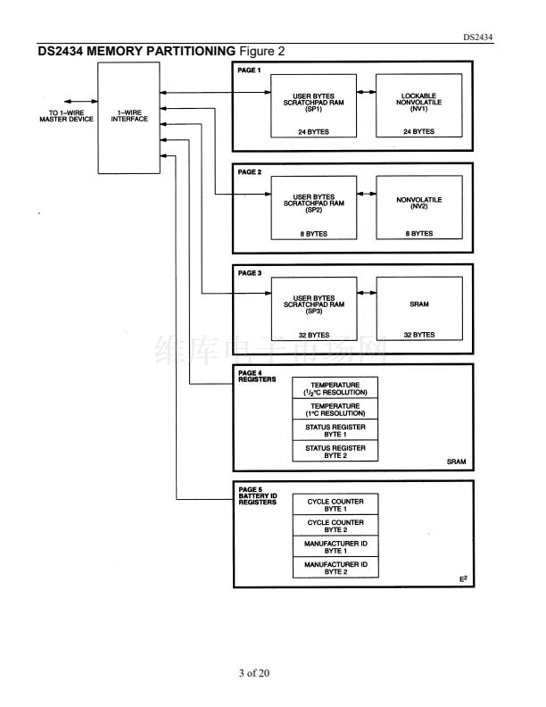
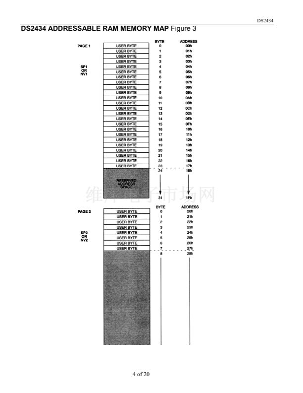
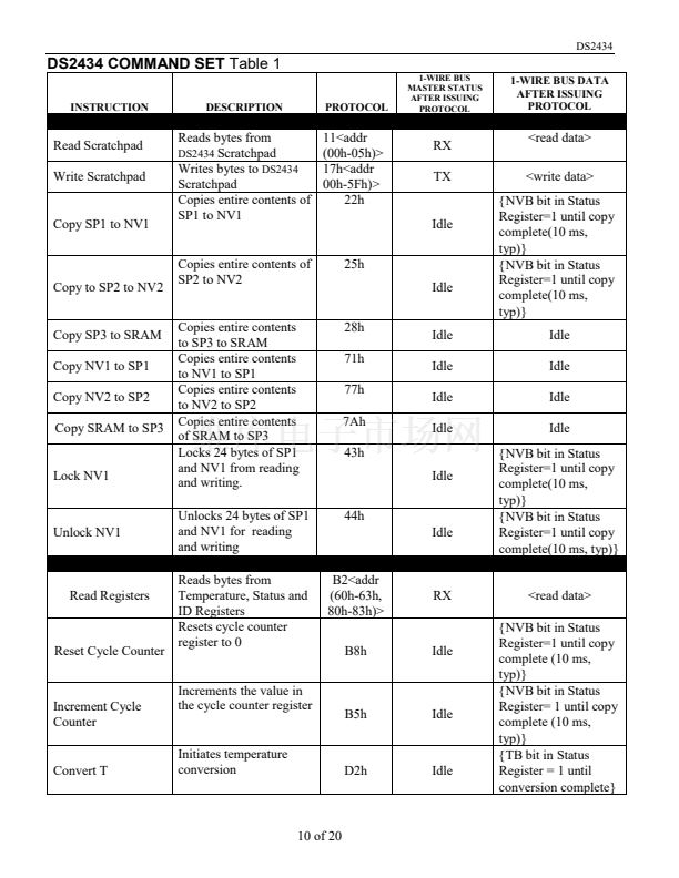
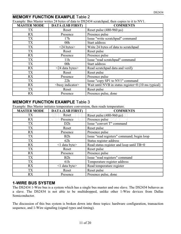
DS2434
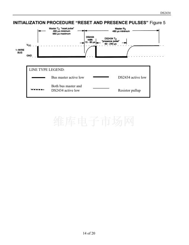
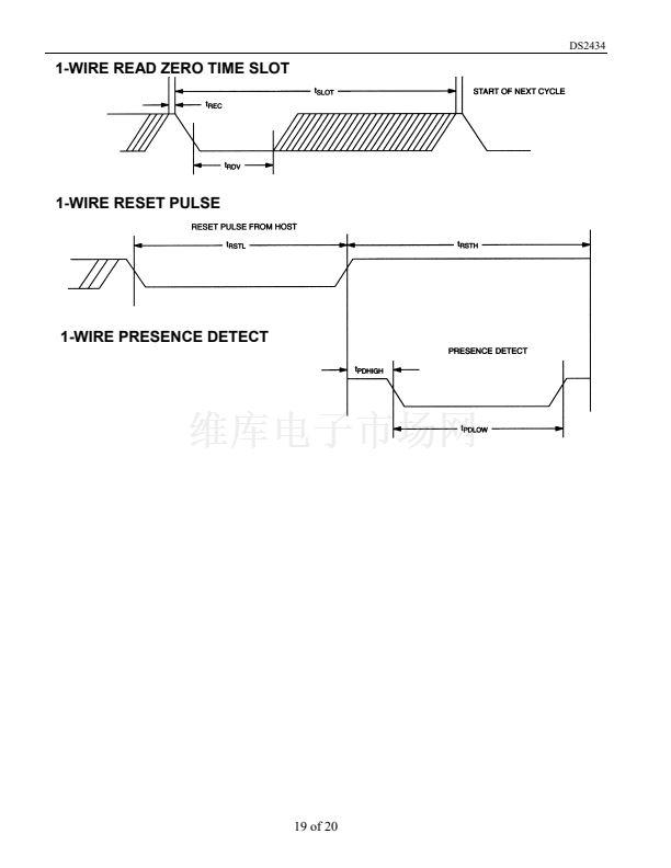
The initialization sequence required to begin any communication with the DS2434 is shown in Figure 5.
A reset pulse followed by a presence pulse indicates the DS2434 is ready to send or receive data given the
correct memory function command.
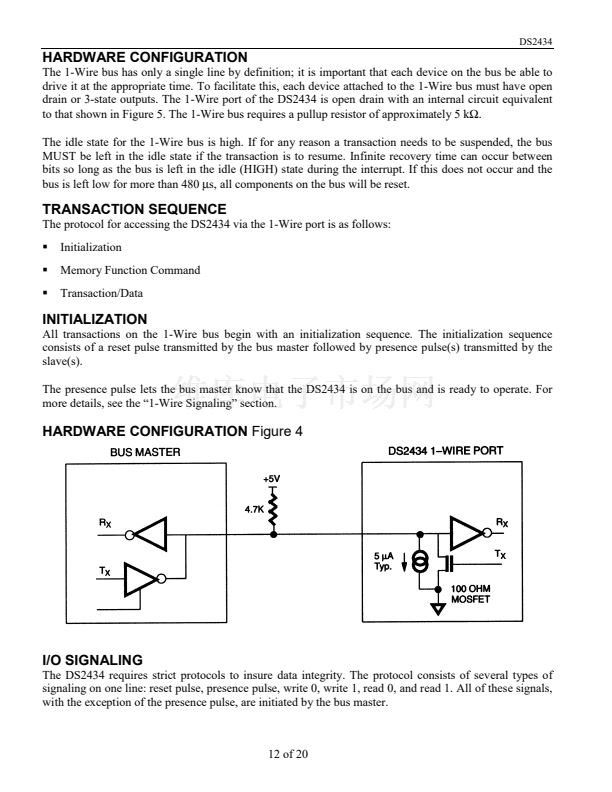
The bus master transmits (TX) a reset pulse (a low signal for a minimum of 480
碌s).
The bus master then
releases the line and goes into a receive mode (RX). The 1-Wire bus is pulled to a high state via the 5k
pullup resistor. After detecting the rising edge on the I/O pin, the DS2434 waits 15-60
碌s
and then
transmits the presence pulse (a low signal for 60-240
碌s).
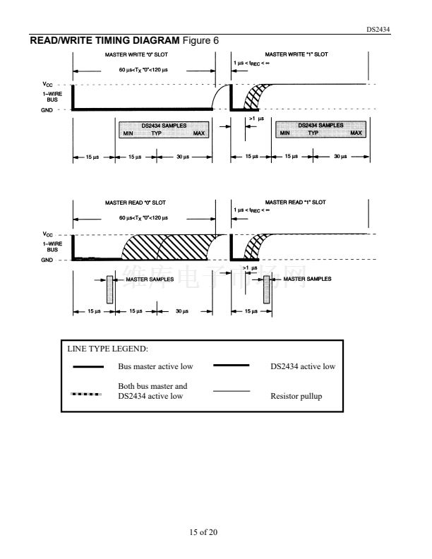
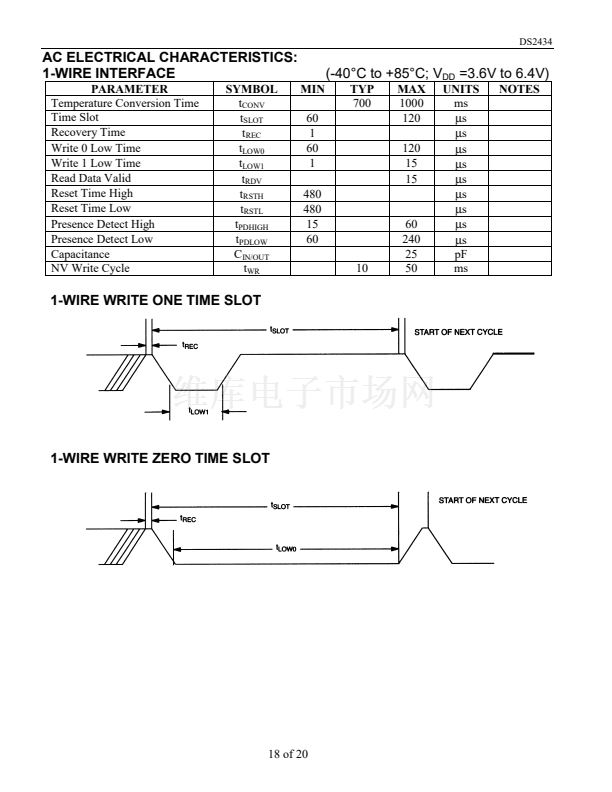
READ/WRITE TIME SLOTS
DS2434 data is read and written through the use of time slots to manipulate bits and a command word to
specify the transaction.
Write Time Slots
A write time slot is initiated when the host pulls the data line from a high logic level to a low logic level.
There are two types of write time slots: Write 1 time slots and Write 0 time slots. All write time slots
must be a minimum of 60
碌s
in duration with a minimum of a 1
碌s
recovery time between individual
write cycles.
The DS2434 samples the I/O line in a window of 15
碌s
to 60
碌s
after the I/O line falls. If the line is high,
a Write 1 occurs. If the line is low, a Write 0 occurs (see Figure 6).
For the host to generate a Write 1 time slot, the data line must be pulled to a logic low level and then
released, allowing the data line to pull up to a high level within 15
碌s
after the start of the write time slot.
For the host to generate a Write 0 time slot, the data line must be pulled to a logic low level and remain
low for the duration of the write time slot.
Read Time Slots
The host generates read time slots when data is to be read from the DS2434. A read time slot is initiated
when the host pulls the data line from a logic high level to logic low level. The data line must remain at a
low logic level for a minimum of 1
碌s;
output data from the DS2434 is then valid for the next 14
碌s
maximum. The host therefore must stop driving the I/O pin low in order to read its state 15
碌s
from the
start of the read slot (see Figure 6). By the end of the read time slot, the I/O pin will pull back high via the
external pullup resistor. All read time slots must be a minimum of 60
碌s
in duration with a minimum of a
1
碌s
recovery time between individual read slots.
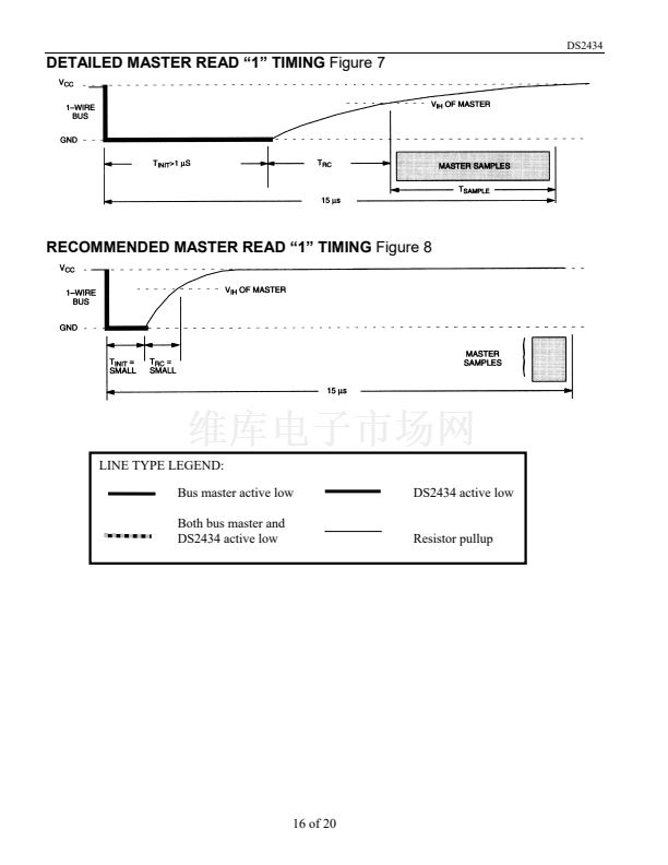
Figure 7 shows that the sum of T
INIT
, T
RC
, and T
SAMPLE
must be less than 15
碌s.
Figure 9 shows that
system timing margin is maximized by keeping T
INIT
and T
RC
as small as possible and by locating the
master sample time towards the end of the 15
碌s
period.
13 of 20


 1
1
 2
2
 3
3
 4
4
 5
5
 6
6
 7
7
 8
8
 9
9
 10
10
 11
11
 12
12
 13
13
 14
14
 15
15
 16
16
 17
17
 18
18
 19
19
 20
20
