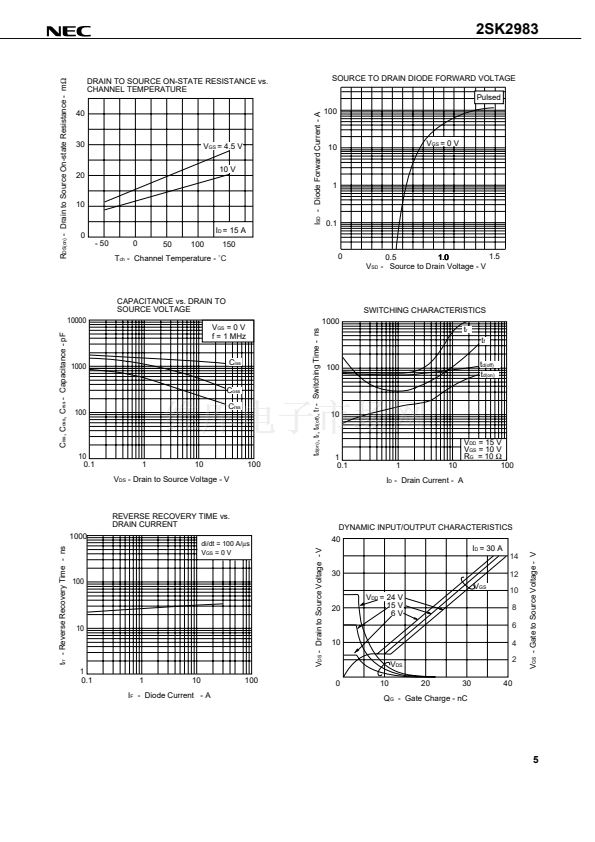
2SK2983
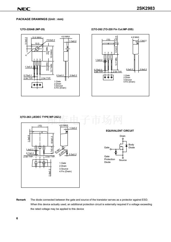
PACKAGE DRAWINGS (Unit : mm)
1)TO-220AB (MP-25)
3.0卤0.3
10.6 MAX.
10.0
5.9 MIN.
15.5 MAX.
4.8 MAX.
2)TO-262 (TO-220 Fin Cut:MP-25S)
1.0卤0.5
蠁
3.6卤0.2
4.8 MAX.
1.3卤0.2
1.3卤0.2
(10)
4
1
2
3
4
1 2 3
6.0 MAX.
1.3卤0.2
1.3卤0.2
12.7 MIN.
12.7 MIN.
8.5卤0.2
0.75卤0.3
2.54 TYP.
0.5卤0.2
2.54 TYP.
1.Gate
2.Drain
3.Source
4.Fin (Drain)
2.8卤0.2
0.75卤0.1
2.54 TYP.
0.5卤0.2
2.54 TYP.
1.Gate
2.Drain
3.Source
4.Fin (Drain)
2.8卤0.2
3)TO-263 (JEDEC TYPE:MP-25ZJ)
4.8 MAX.
1.3卤0.2
4
1.0卤0.5
8.5卤0.2
(10)
EQUIVALENT CIRCUIT
Drain
5.7卤0.4
1.4卤0.2
0.7卤0.2
2.54 TYP. 1
2
(
R)
0.5
Gate
.8R
)
0.5卤0.2
Body
Diode
3 2.54 TYP.
(0
Remark
The diode connected between the gate and source of the transistor serves as a protector against ESD.
When this device actually used, an additional protection circuit is externally required if a voltage exceeding
the rated voltage may be applied to this device
6
2.8卤0.2
1.Gate
2.Drain
3.Source
4.Fin (Drain)
Gate
Protection
Diode
Source


 1
1
 2
2
 3
3
 4
4
 5
5
 6
6
 7
7
 8
8
