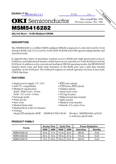
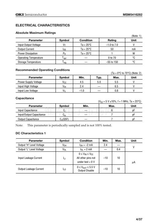
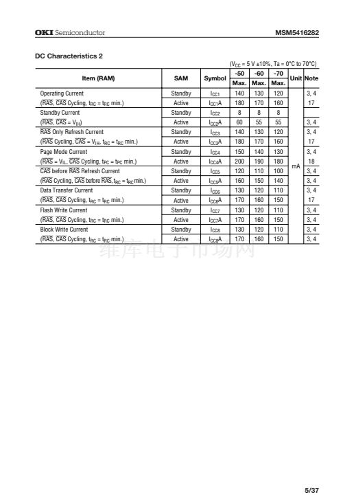
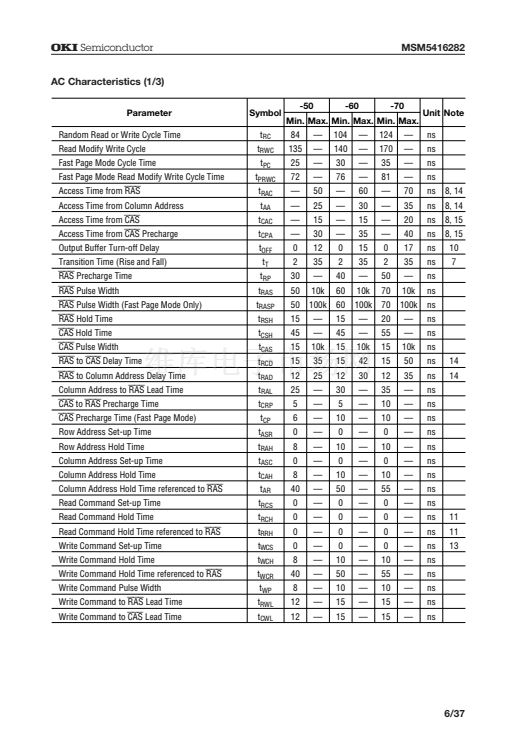
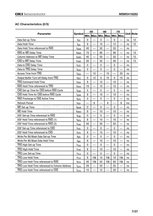
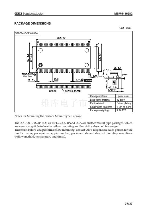
隆 Semiconductor
MSM5416282
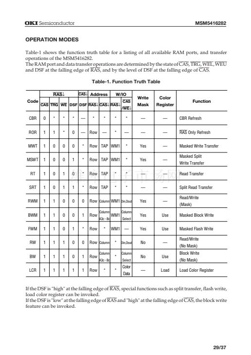
RAM PORT OPERATION
RAM Read Cycle:
RAS
falling edge ---
TRG
=
CAS
= "H", DSF = "L"
CAS
falling edge --- DSF = "L"
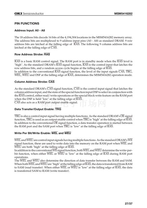
Row address is entered at the falling edge of
RAS
and column address at the falling edge of
CAS
to the device as in conventional DRAM. When both
WEL
and
WEU
are "high" and
TRG
is "low"
while
CAS
is "low", the data outputs through DQ pins.
RAM Write Cycle:
RAS
falling edge ---
TRG
=
CAS
= "H", DSF = "L"
CAS
falling edge --- DSF = "L"
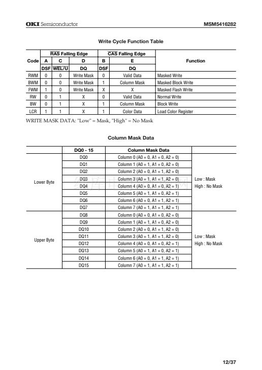
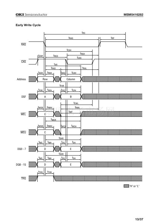
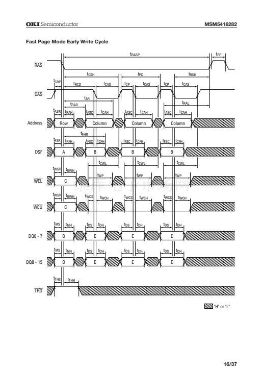
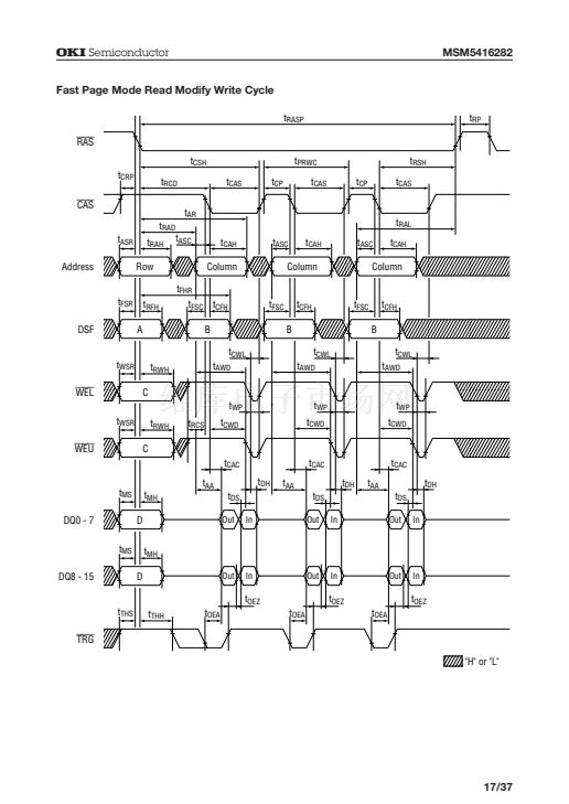
1) Write cycle with no mask:
RAS
falling edge --
WEL
=
WEU
= "H"
If either
WEL
or
WEU
is set "low" at the falling edge of
CAS
after
RAS
goes "low", a write cycle
is excuted. If either
WEL
or
WEU
is set "low" before the
CAS
falling edge, this cycle becomes an
early write cycle, and all DQ pins attain high impedance.
If either
WEL
or
WEU
is "low" when
CAS
goes "low", the write affects only those corresponding
8 bits with the latched data.
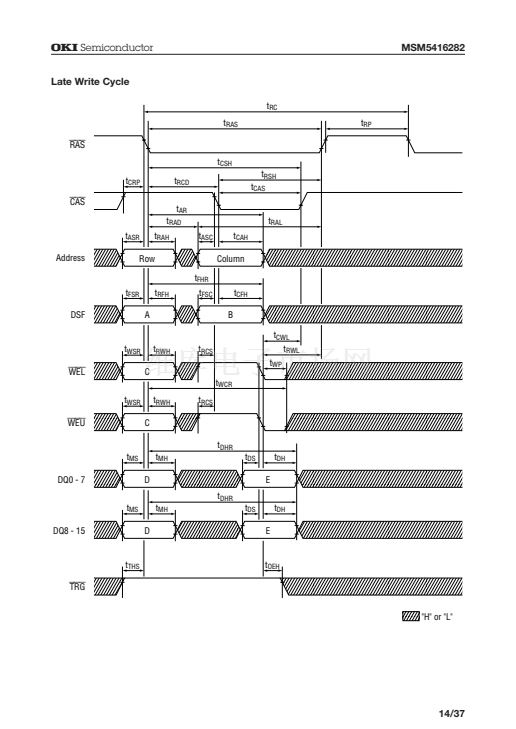
If both
WEL
and
WEU
are set "low" after the
CAS
falling edge, this cycle becomes a late write
cycle, and all 16 data are latched on the falling edge of
WEL
or
WEU.
Byte write occurs if either
WEL
or
WEU
falls during the cycle. DQ pins don't achieve high
impedance in this cycle, so data should be entered with
TRG
in "high".
2) Write cycle with mask:
RAS
falling edge --
WEL
or
WEU
= "L"
If either
WEL
or
WEU
is set "low" at the falling edge of
RAS,
the mask write mode can be invoked.
Mask data is loaded and used. The mask data on DQ0 - DQ15 is latched into the write mask
register at the falling edge of
RAS.
When the mask data is low, writing is inhibited into the RAM
and the mask data is high, data is written into the RAM. This mask data is in effect during the
RAS
cycle. In page mode cycle the mask data is retained during page access.
30/37


 1
1
 2
2
 3
3
 4
4
 5
5
 6
6
 7
7
 8
8
 9
9
 10
10
 11
11
 12
12
 13
13
 14
14
 15
15
 16
16
 17
17
 18
18
 19
19
 20
20
 21
21
 22
22
 23
23
 24
24
 25
25
 26
26
 27
27
 28
28
 29
29
 30
30
 31
31
 32
32
 33
33
 34
34
 35
35
 36
36
 37
37
