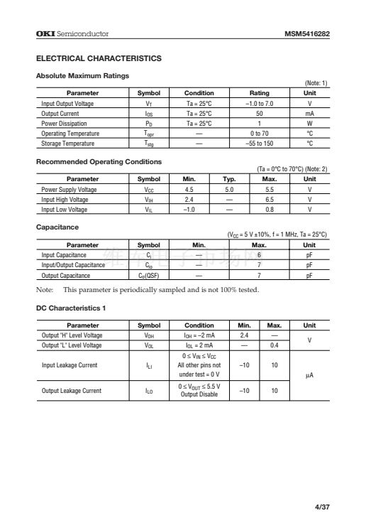
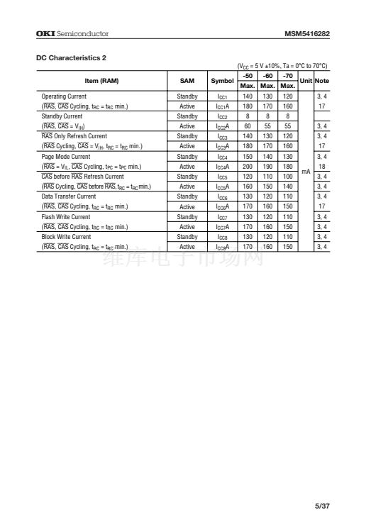
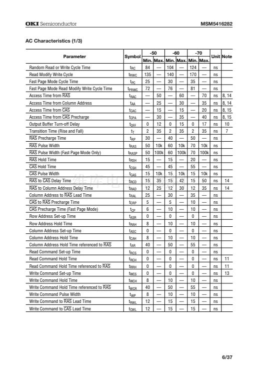
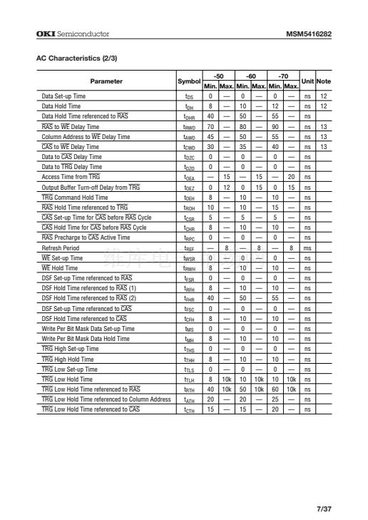
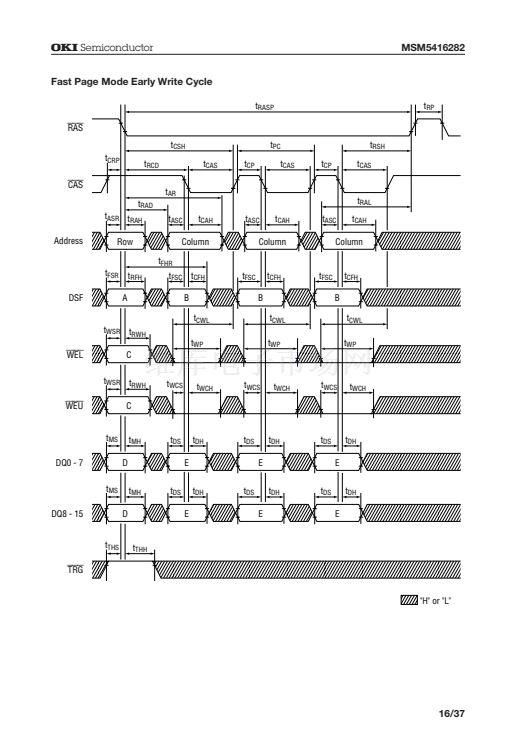
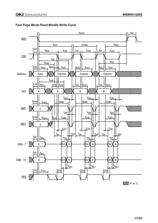
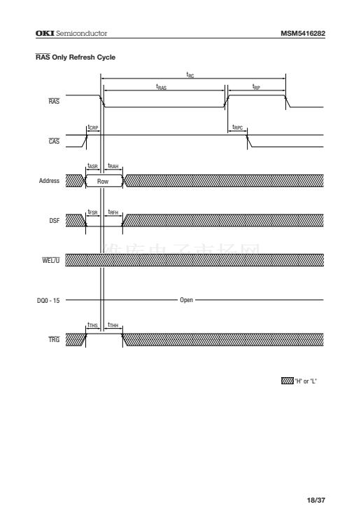
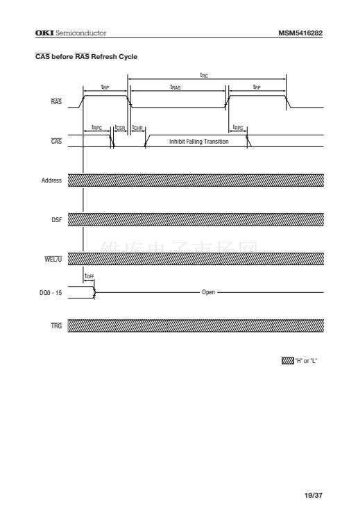
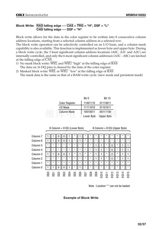
隆 Semiconductor
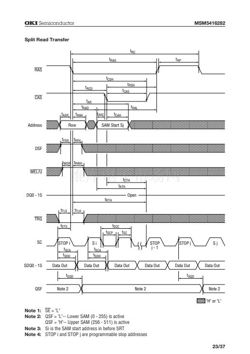
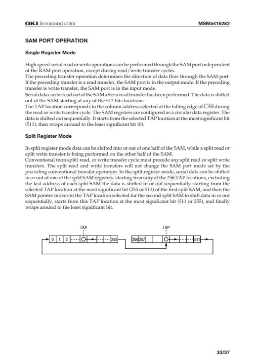
Split Data Transfer and QSF
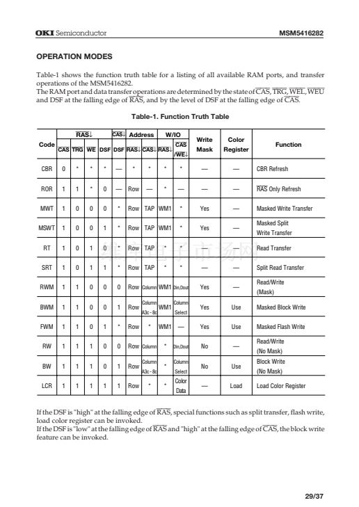
MSM5416282
The MSM5416282 features a bidirectional split data transfer capability between the RAM and
SAM. During split data transfer operation, the serial register is split into two halves which can
be controlled independently. Split read or split write transfer operation can be performed to or
from one half of the serial register, while serial data can be shifted into or out of the other half of
the serial register. The most significant column address location (A8C) is controlled internally to
determine which half of the serial register will be reloaded from the RAM. QSF is an output
which indicates which half of the serial register is in an active state. QSF changes state when the
last SC clock is applied to active split SAM.
Split Read Transfer:
RAS
falling edge ---
CAS
=
WEL
=
WEU
= DSF = "H",
TRG
= "L"
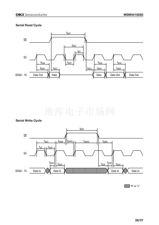
Split read transfer consists of loading 256 words by 16 bits of data from a selected row of the split
RAM into the corresponding non-active split SAM register. Serial data can be shifted out from
the other half of the split SAM register simultaneously. During split read transfer operation, the
RAM port input clocks do not have to be synchronized with the serial clock SC, thus eliminating
timing restrictions as in the case of real time read transfers. A split read transfer can be performed
after a delay of t
STS
from the change of state of the QSF output is satisfied.
Conventional (non-split) read transfer operation must precede split read transfer cycles.
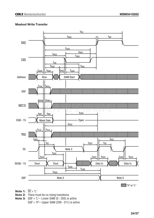
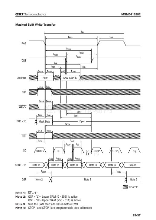
Masked Split Write Transfer:
RAS
falling edge ---
CAS
= DSF = "H",
TRG
= "L"
WEL
or
WEU
= "L"
Split write transfer consists of loading 256 words by 16 bits of data from the non-active split SAM
register into a selected row of the corresponding split RAM. Serial data can be shifted into the
other half of the split SAM register simultaneously. During split write transfer operation, the
RAM port input clocks do not have to be synchronized with the serial clock SC, thus allowing
for real time transfer. This write transfer operation, which is the same as a mask write operation
in RAM, can be selectively controlled for 16 DQis by inputing the mask data from DQ0 - DQ15
at the falling edge of
RAS.
A split write transfer can be performed after a delay of t
STS
from the change of state of the QSF
output is satisfied.
A masked write transfer operation must precede split write transfer. The purpose is to switch the
SAM port from output mode to input mode, and to set the initial TAP location prior to split write
transfer operations.
POWER UP
Power must be applied to the
RAS
and
TRG
input signals to pull them "high" before, or at the
same time as, the V
CC
supply is turned on. After power-up, a pause of 200
ms
minimum is
required with
RAS
and
TRG
held "high". After the pause, a minimum of 8
RAS
and 8 SC dummy
cycles must be performed to stabilize the internal circuitry, before valid read, write or transfer
operations can begin. During the initialization period, the
TRG
signal must be held "high". If the
internal refresh counter is used, a minimum 8
CAS
before
RAS
cycles are required instead of 8
RAS
cycles.
(NOTE) INITIAL STATE AFTER POWER UP
The initial state can not be guaranteed for various power up conditions and input signal levels.
Therefore, it is recommended that the initial state be set after the initialization of the device is
performed and before valid operations begin.
36/37


 1
1
 2
2
 3
3
 4
4
 5
5
 6
6
 7
7
 8
8
 9
9
 10
10
 11
11
 12
12
 13
13
 14
14
 15
15
 16
16
 17
17
 18
18
 19
19
 20
20
 21
21
 22
22
 23
23
 24
24
 25
25
 26
26
 27
27
 28
28
 29
29
 30
30
 31
31
 32
32
 33
33
 34
34
 35
35
 36
36
 37
37
