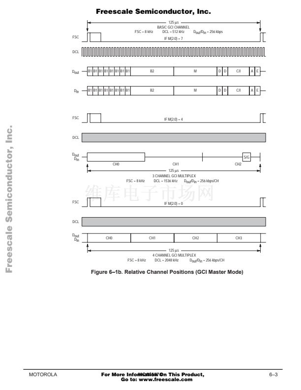
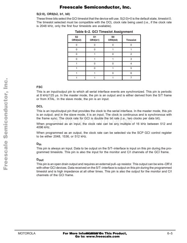
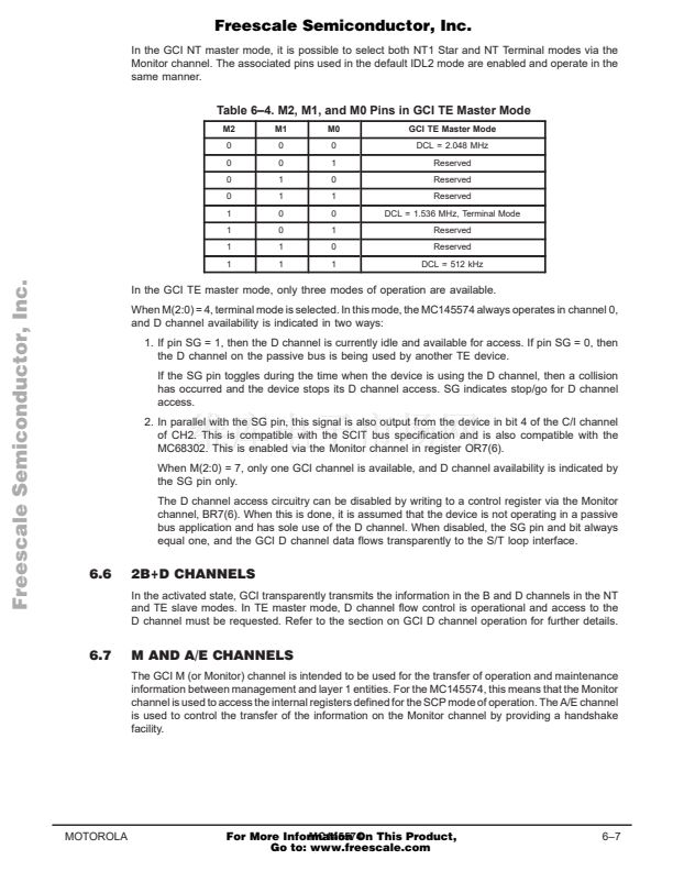
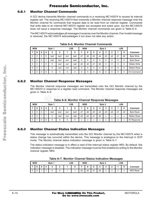
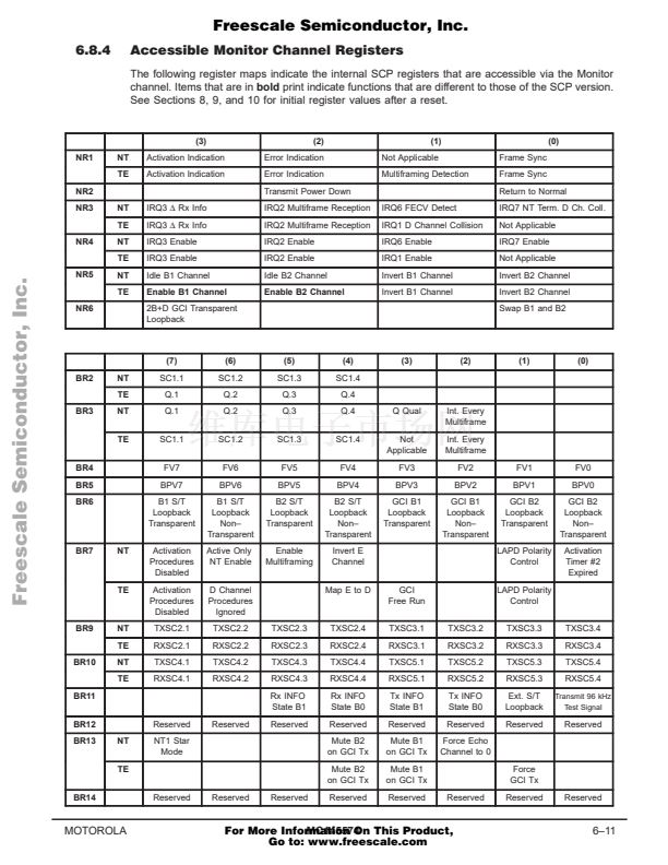
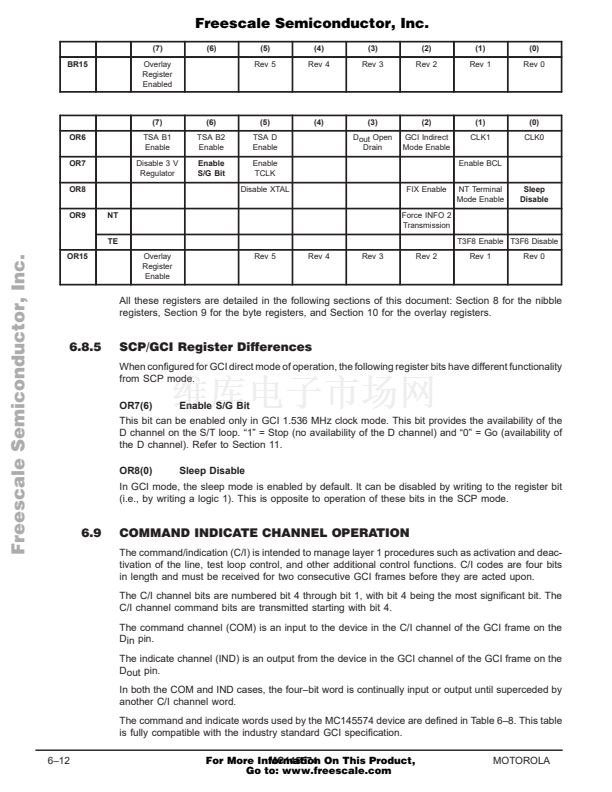
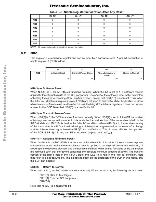
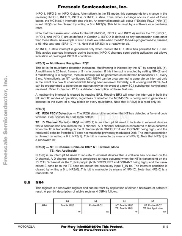
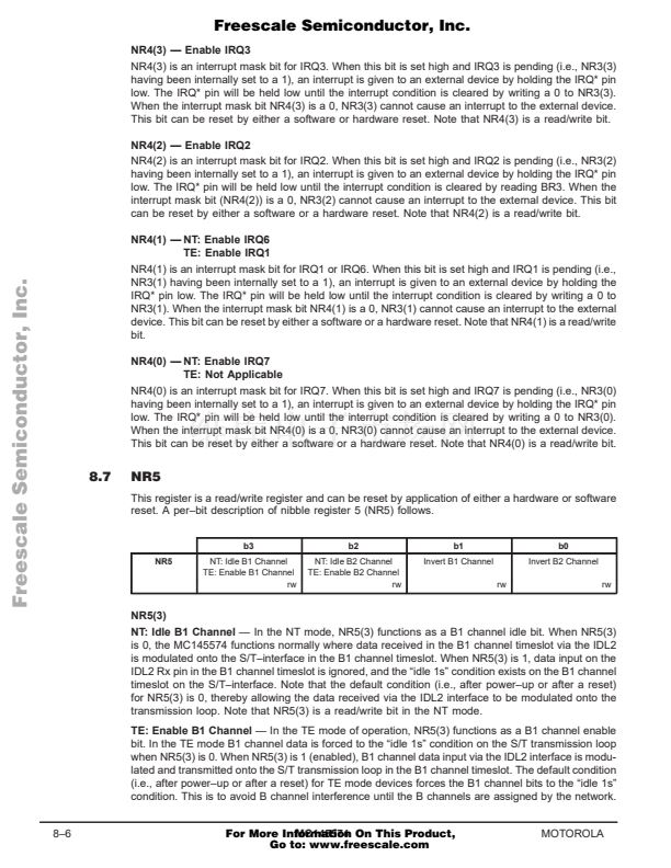
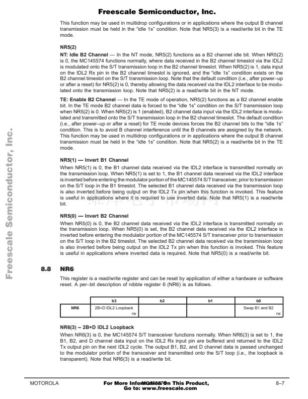
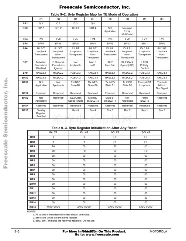
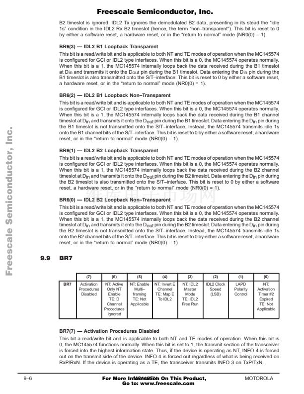
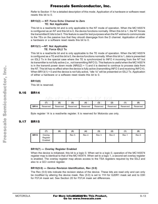
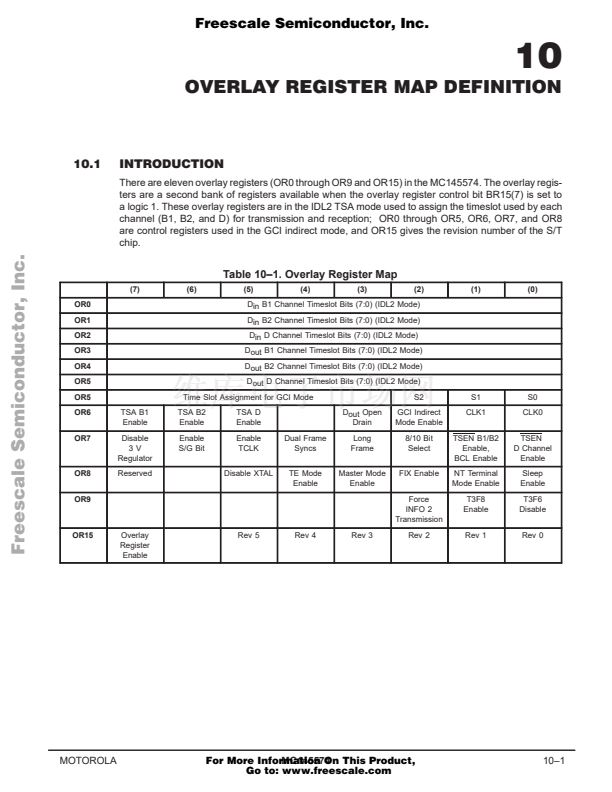
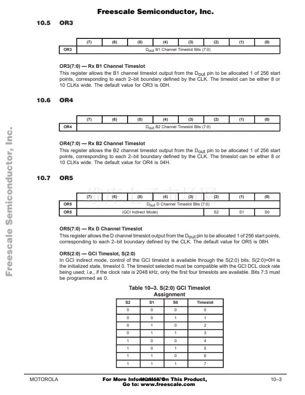
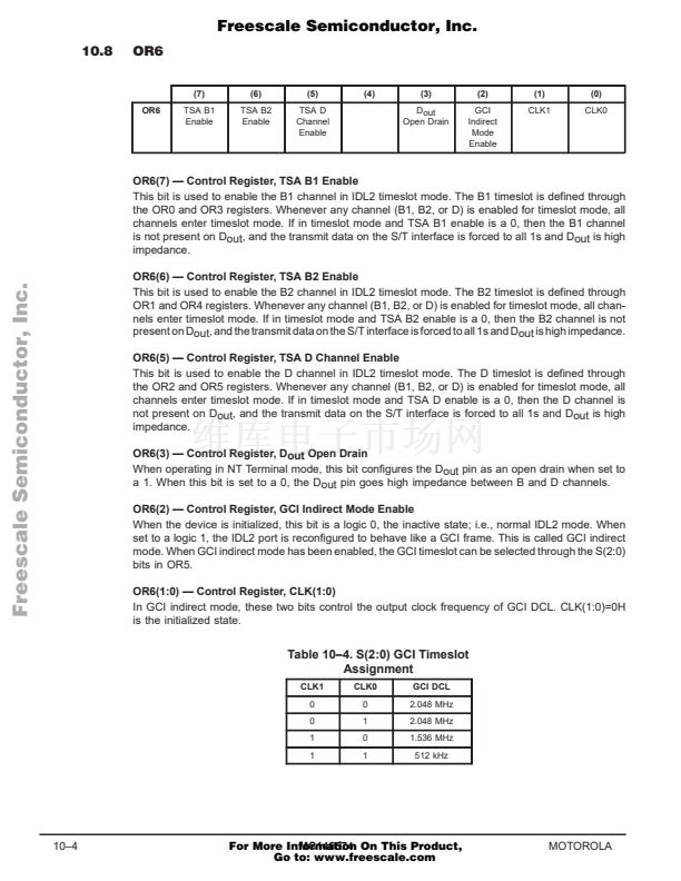
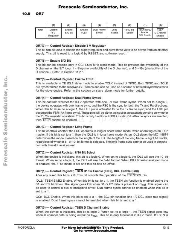
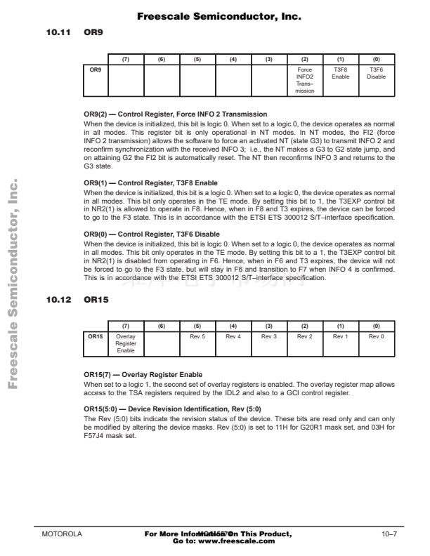
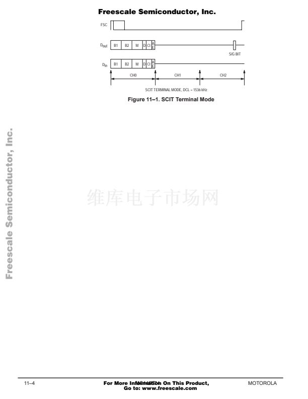
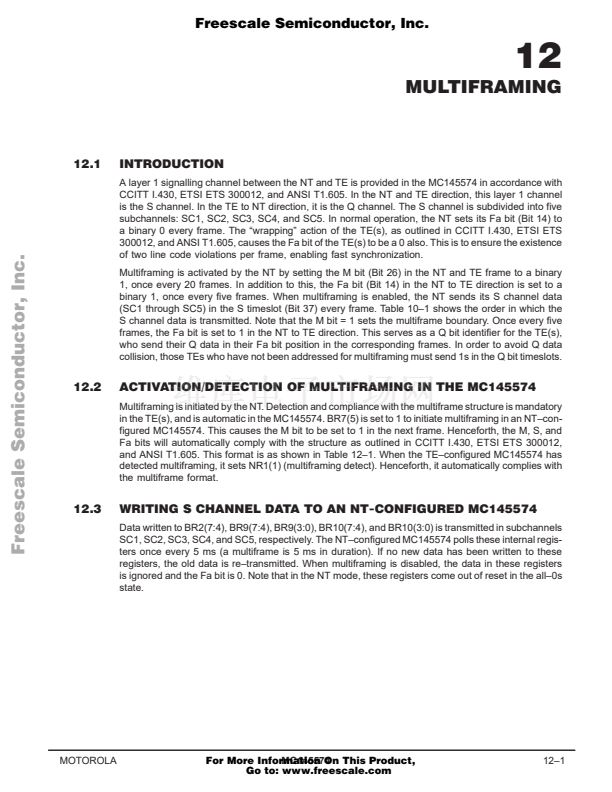
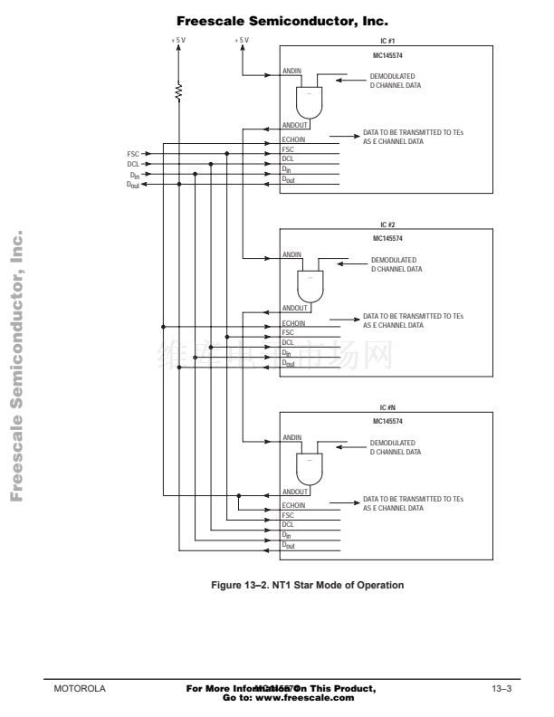
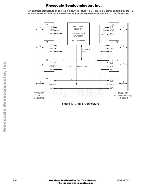
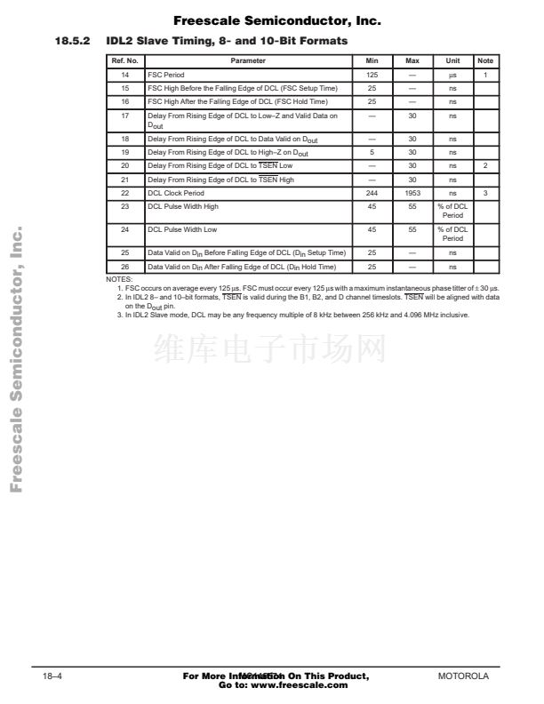
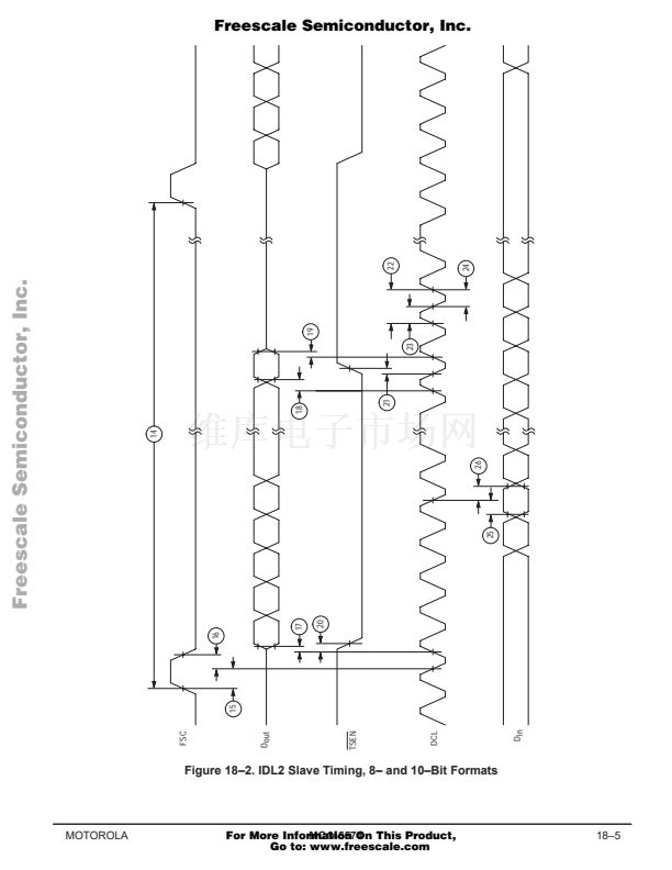
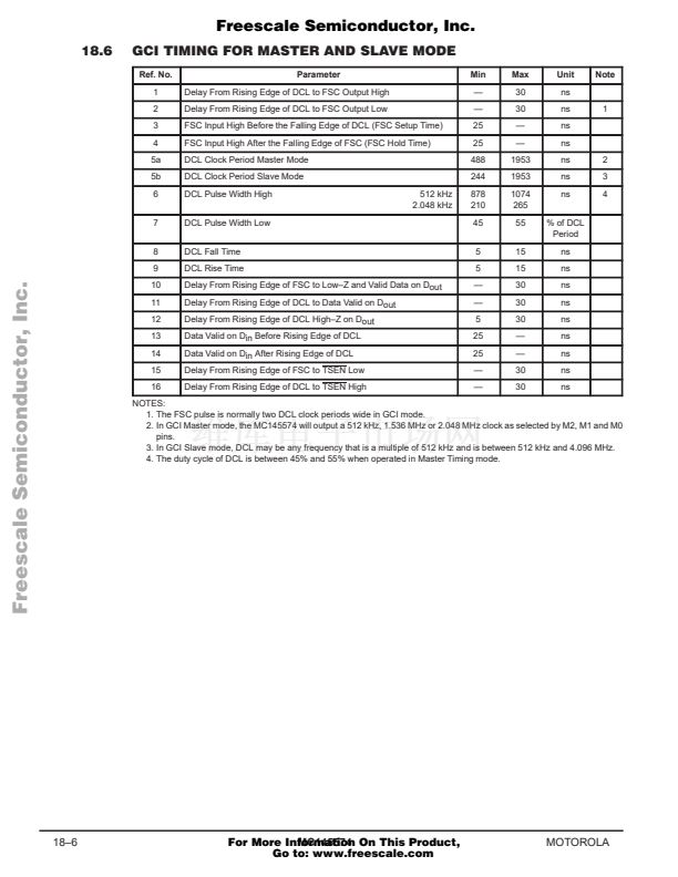
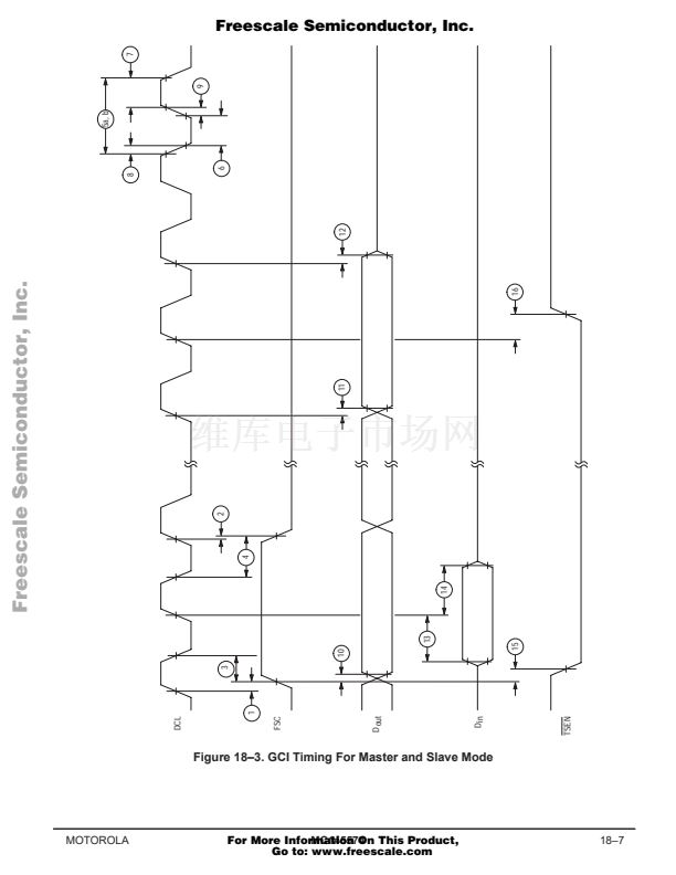
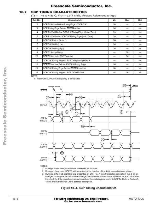
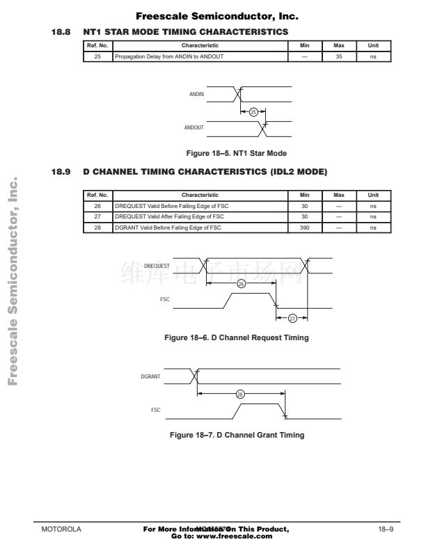
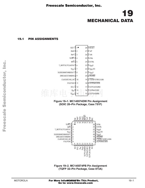
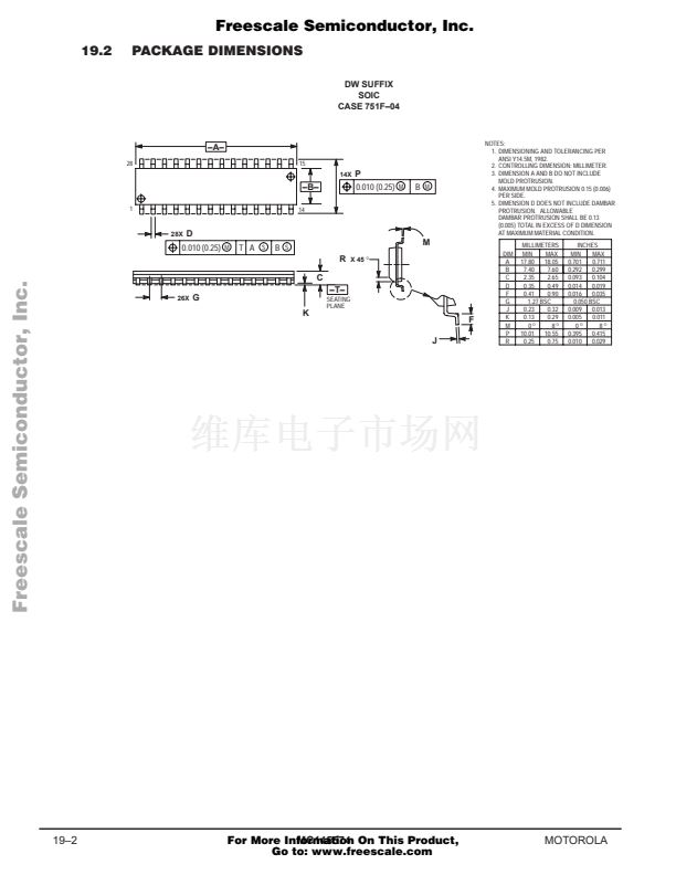
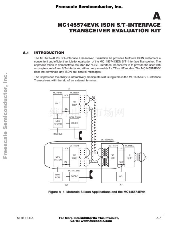
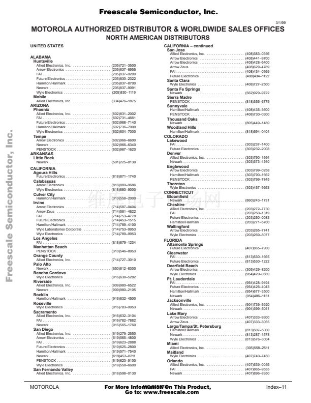
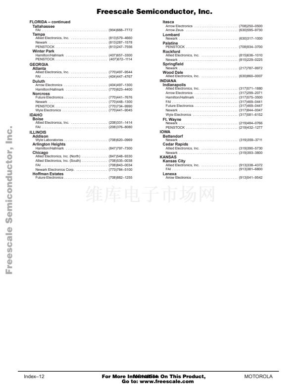
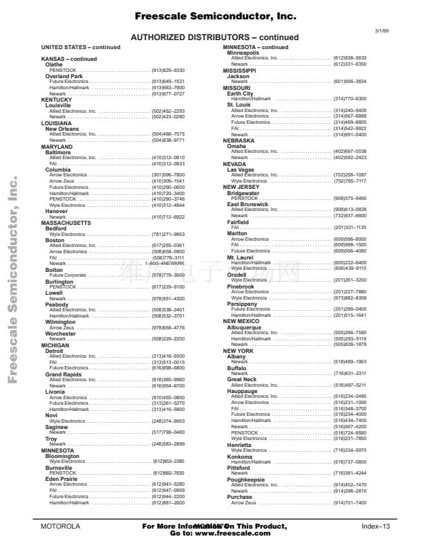
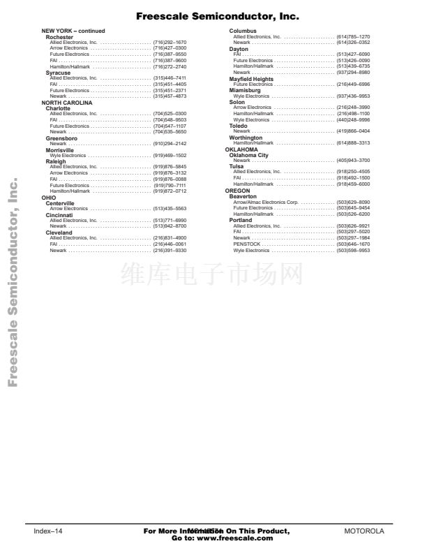
Freescale Semiconductor, Inc.
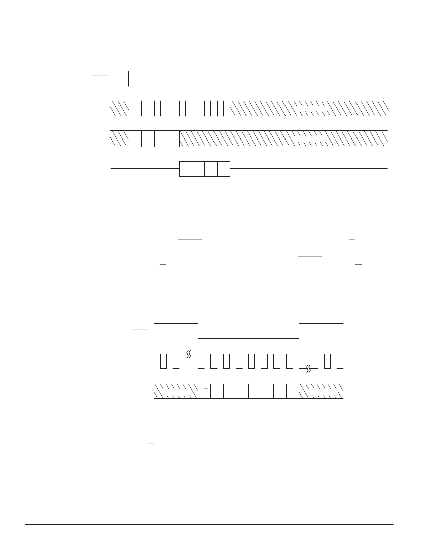
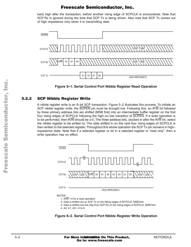
back high after the transaction, before another rising edge of SCPCLK is encountered. Note that
SCP Rx is ignored during the time that SCP Tx is being driven. Also note that SCP Tx comes out
of high impedance only when it is transmitting data.
SCPEN
SCPCLK
DON鈥橳 CARE
SCP Rx
R/W
A2
A1
A0
DON鈥橳 CARE
Freescale Semiconductor, Inc...
SCP Tx
D3
D2 D1
D0
HIGH IMPEDANCE
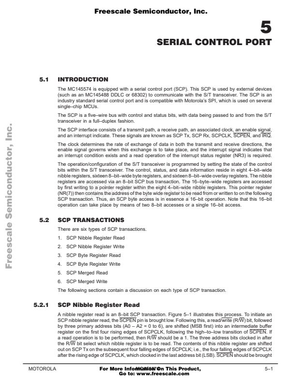
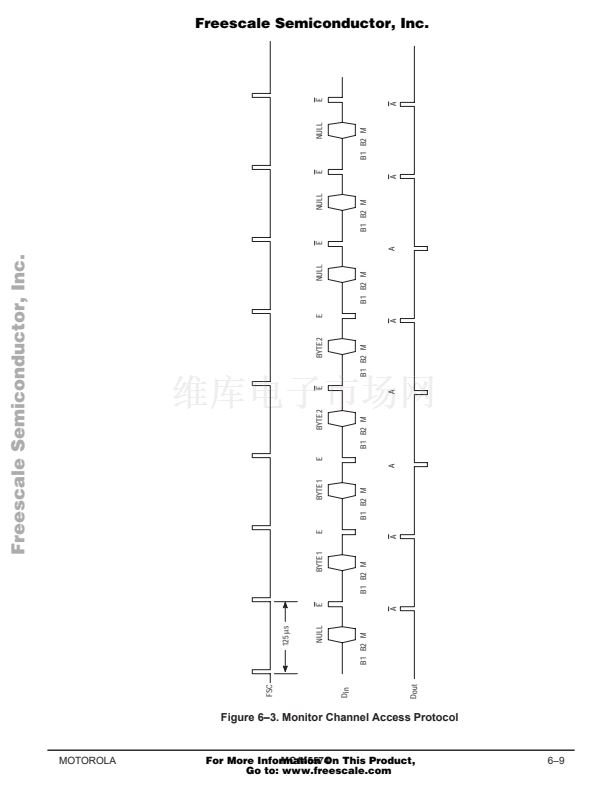
Figure 5鈥?. Serial Control Port Nibble Register Read Operation
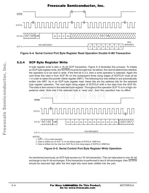
5.2.2
SCP Nibble Register Write
A nibble register write is an 8鈥揵it SCP transaction. Figure 5鈥? illustrates this process. To initiate an
SCP nibble register write, the SCPEN pin must be brought low. Following this, an R/W bit followed
by three primary address bits are shifted (MSB first) into an intermediate buffer register on the first
four rising edges of SCPCLK following the high鈥搕o鈥搇ow transition of SCPEN. If a write operation is
to be performed, then R/W should be a 0. The three address bits, clocked in after the R/W bit, select
the nibble register to be written to. The data shifted in on the next four rising edges of SCPCLK is
then written to the selected register. Throughout this whole operation the SCP Tx pin remains in high鈥?/div>
impedance state. Note that if a selected register or bit in a selected register is 鈥渞ead only鈥? then a
write operation has no effect.
SCPEN
SCPCLK
SCP Rx
DON鈥橳 CARE
R/W A2
A1
A0
D3
D2
D1
D0
DON鈥橳 CARE
SCP Tx
HIGH IMPEDANCE
NOTES:
1. R/W = 0 for a read operation.
2. Data is shifted out on SCP Tx on the falling edges of SCPCLK, MSB first.
3. Data is shifted into the chip from SCP Rx on the rising edges of SCPCLK, MSB first.
4. A2, A1, A0 = 0 to 6.
Figure 5鈥?. Serial Control Port Nibble Register Write Operation
5鈥?
MC145574
For More Information On This Product,
Go to: www.freescale.com
MOTOROLA


 1
1
 2
2
 3
3
 4
4
 5
5
 6
6
 7
7
 8
8
 9
9
 10
10
 11
11
 12
12
 13
13
 14
14
 15
15
 16
16
 17
17
 18
18
 19
19
 20
20
 21
21
 22
22
 23
23
 24
24
 25
25
 26
26
 27
27
 28
28
 29
29
 30
30
 31
31
 32
32
 33
33
 34
34
 35
35
 36
36
 37
37
 38
38
 39
39
 40
40
 41
41
 42
42
 43
43
 44
44
 45
45
 46
46
 47
47
 48
48
 49
49
 50
50
 51
51
 52
52
 53
53
 54
54
 55
55
 56
56
 57
57
 58
58
 59
59
 60
60
 61
61
 62
62
 63
63
 64
64
 65
65
 66
66
 67
67
 68
68
 69
69
 70
70
 71
71
 72
72
 73
73
 74
74
 75
75
 76
76
 77
77
 78
78
 79
79
 80
80
 81
81
 82
82
 83
83
 84
84
 85
85
 86
86
 87
87
 88
88
 89
89
 90
90
 91
91
 92
92
 93
93
 94
94
 95
95
 96
96
 97
97
 98
98
 99
99
 100
100
 101
101
 102
102
 103
103
 104
104
 105
105
 106
106
 107
107
 108
108
 109
109
 110
110
 111
111
 112
112
 113
113
 114
114
 115
115
 116
116
 117
117
 118
118
 119
119
 120
120
 121
121
 122
122
 123
123
 124
124
 125
125
 126
126
 127
127
 128
128
 129
129
 130
130
 131
131
 132
132
 133
133
 134
134
 135
135
 136
136
 137
137
 138
138
 139
139
 140
140
 141
141
 142
142
 143
143
 144
144
 145
145
 146
146
 147
147
 148
148
 149
149
 150
150
 151
151
 152
152
 153
153
 154
154
 155
155
 156
156
 157
157
 158
158
 159
159
 160
160
 161
161
 162
162
 163
163
 164
164
