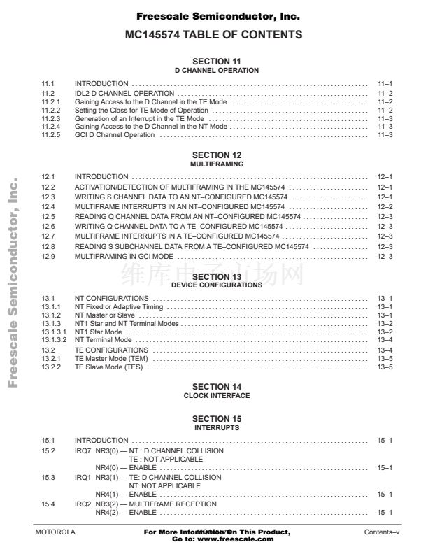
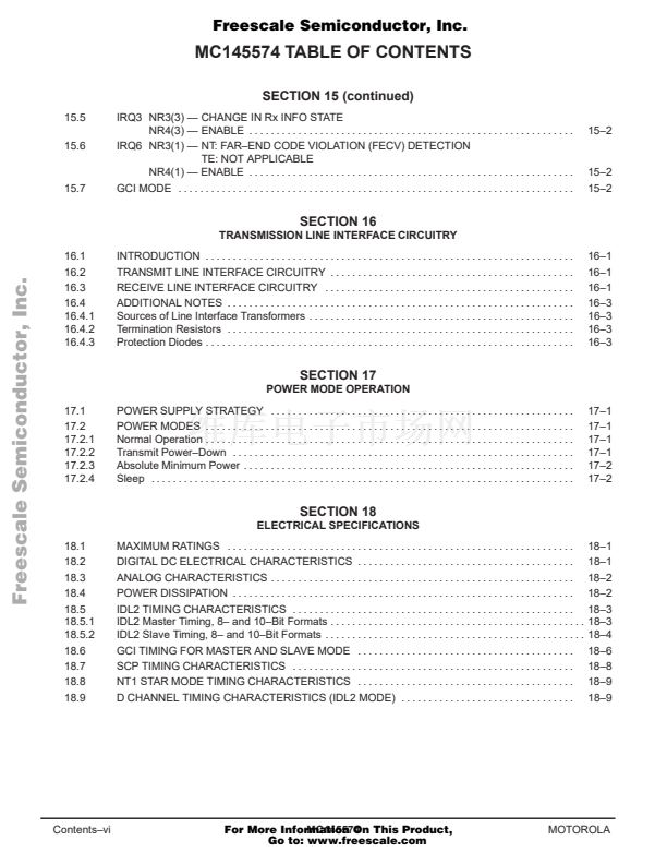
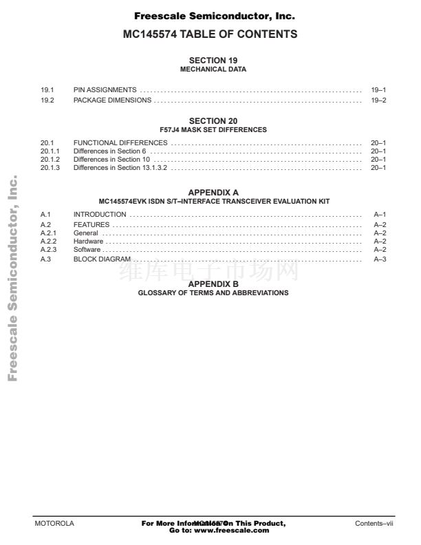
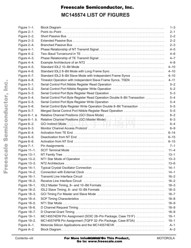
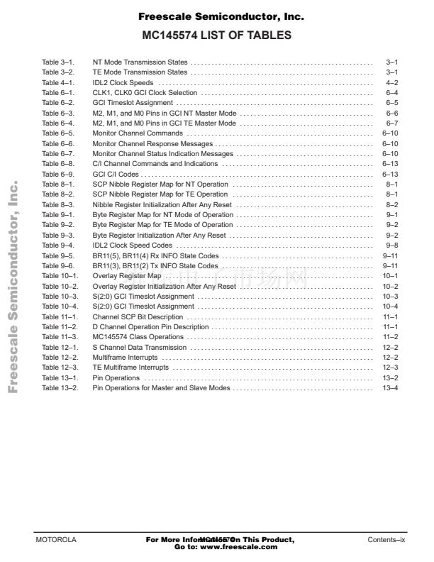
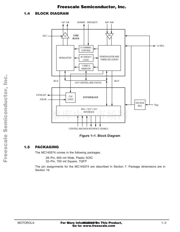
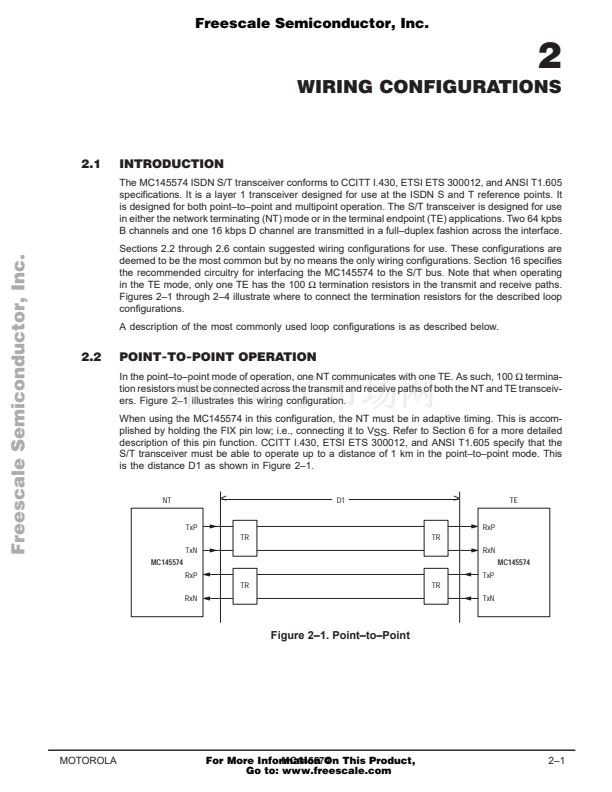
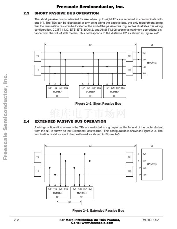
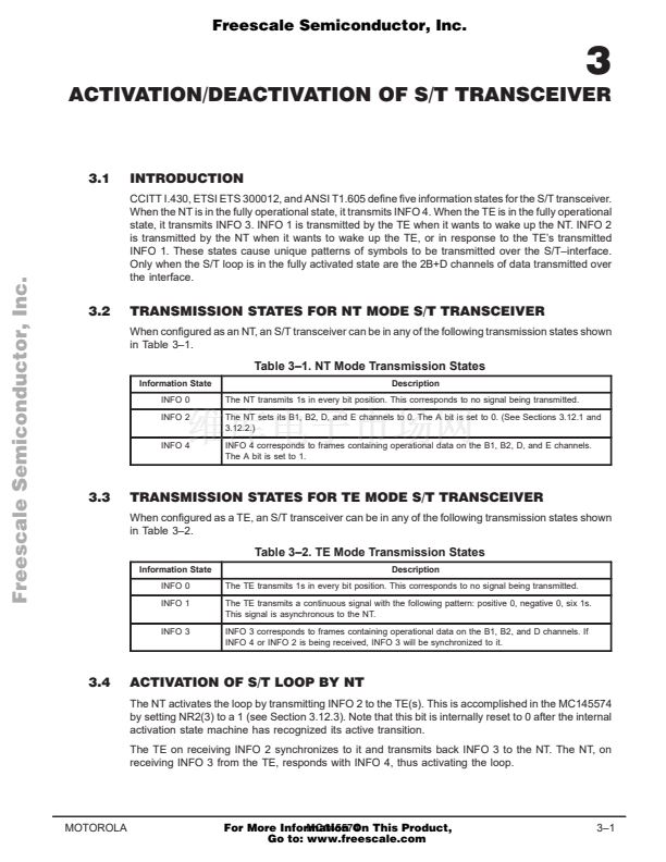
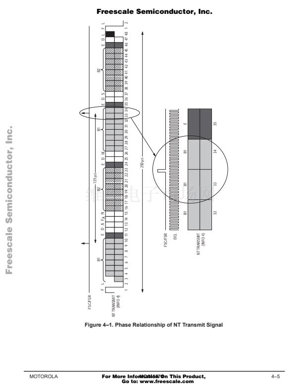
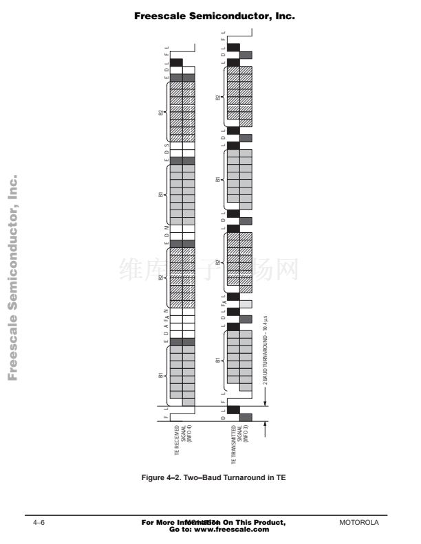
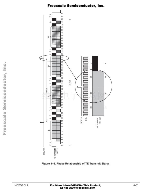
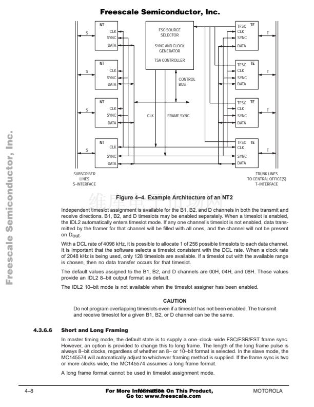
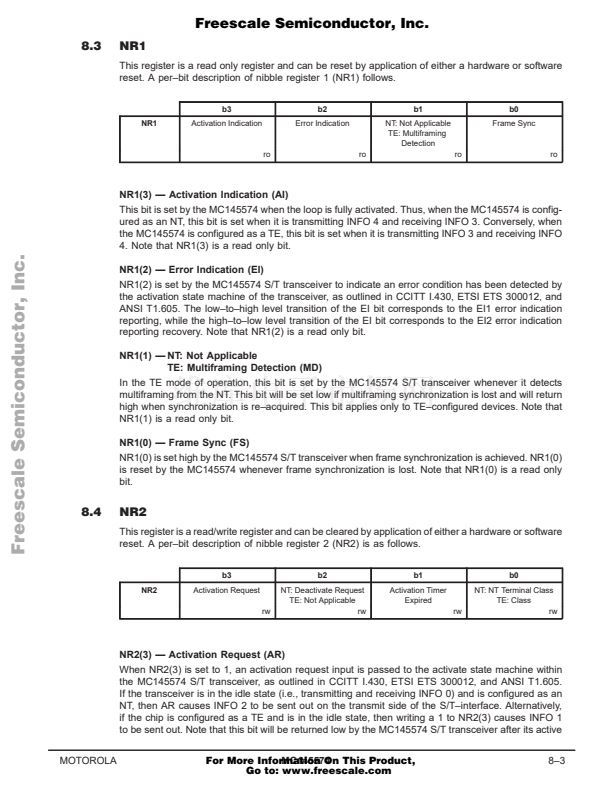
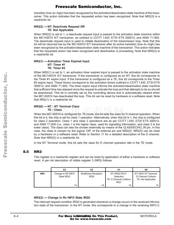
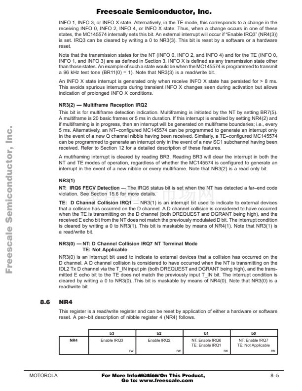
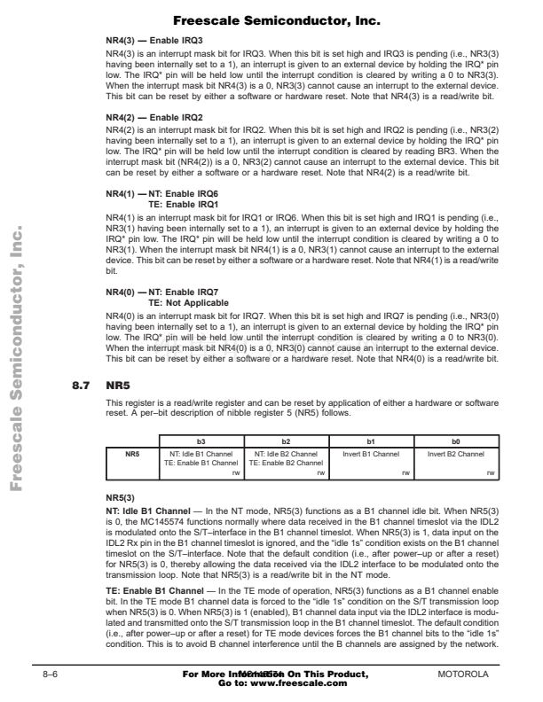
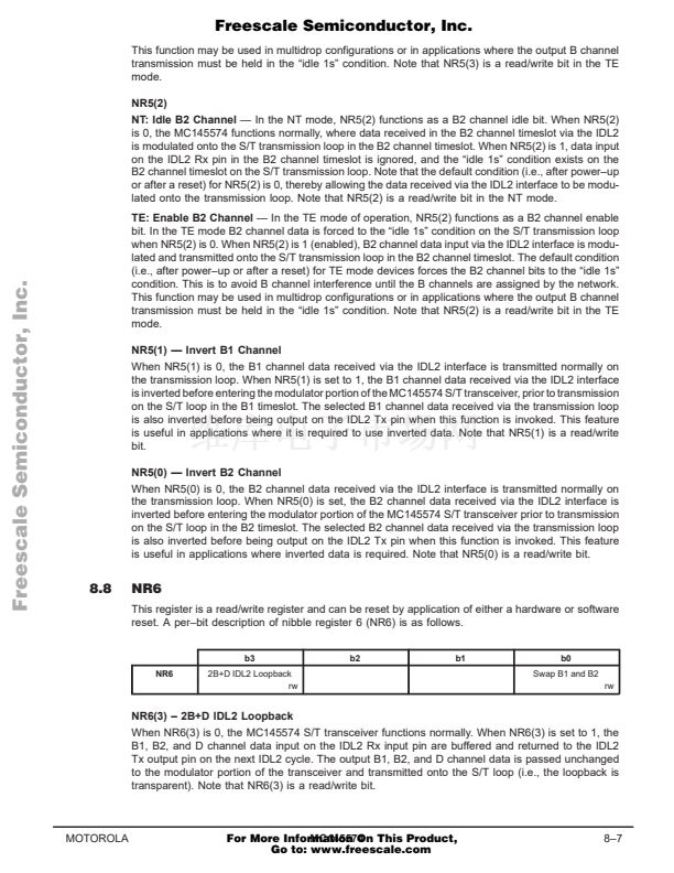
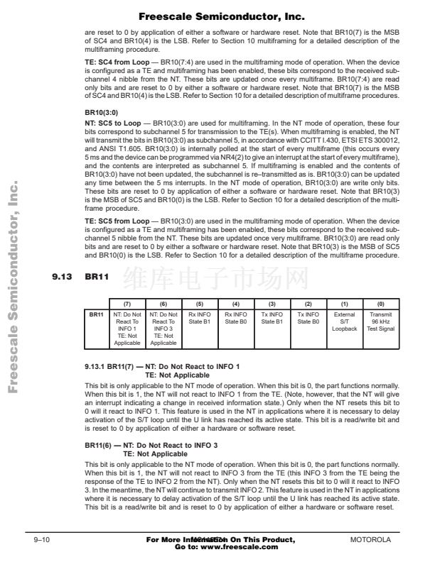
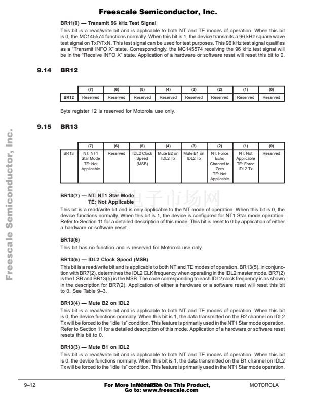
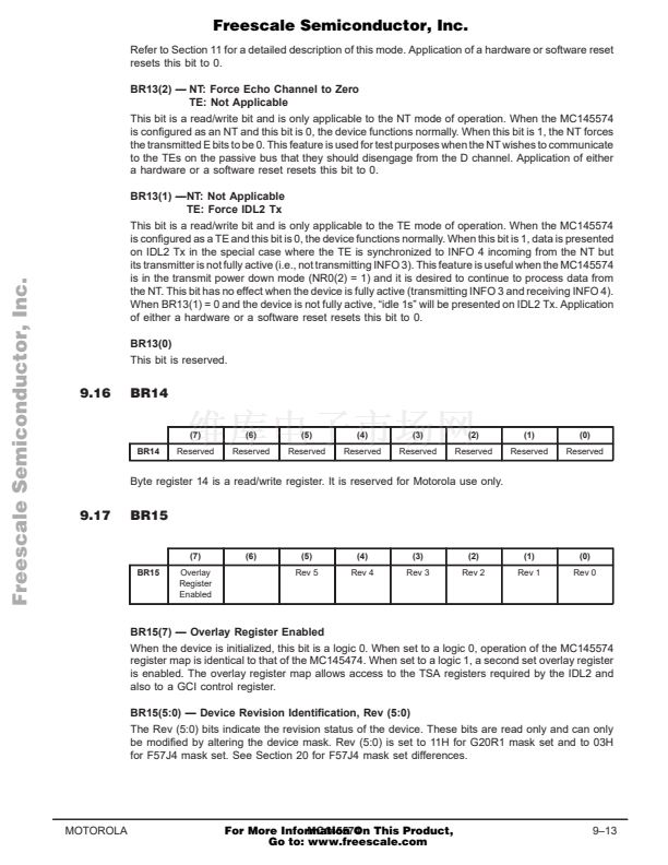
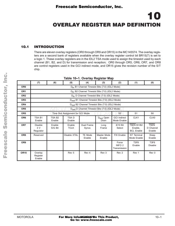
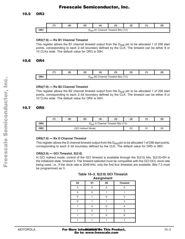
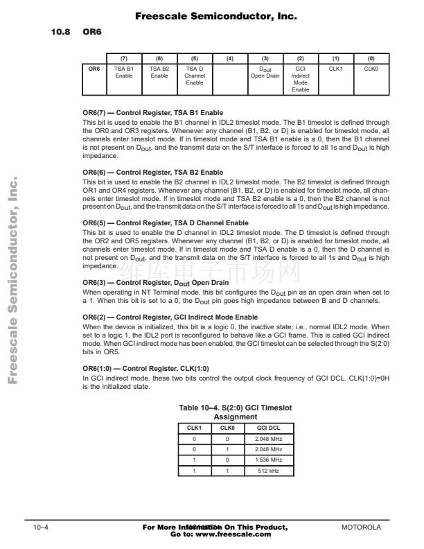
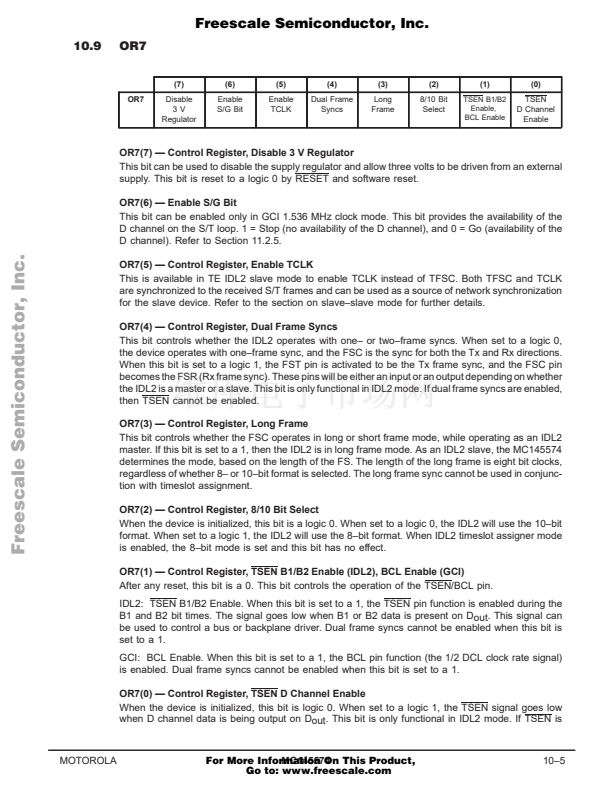
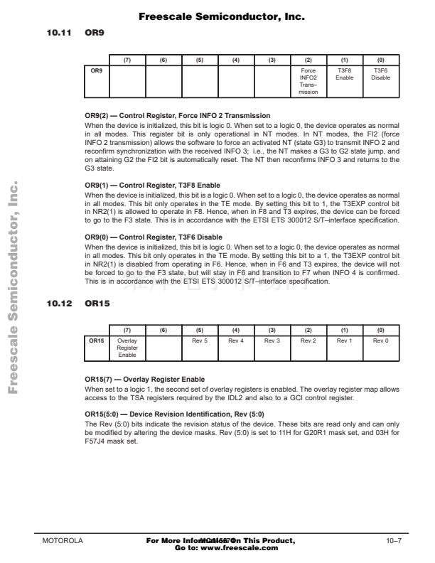
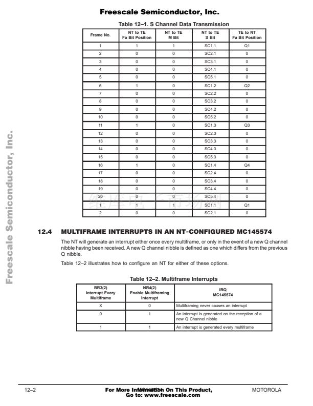
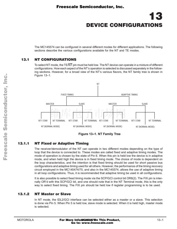
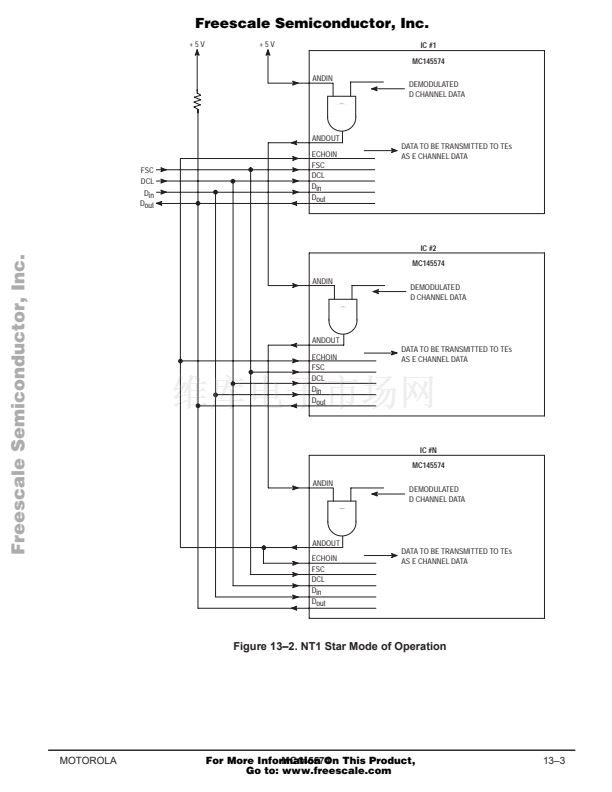
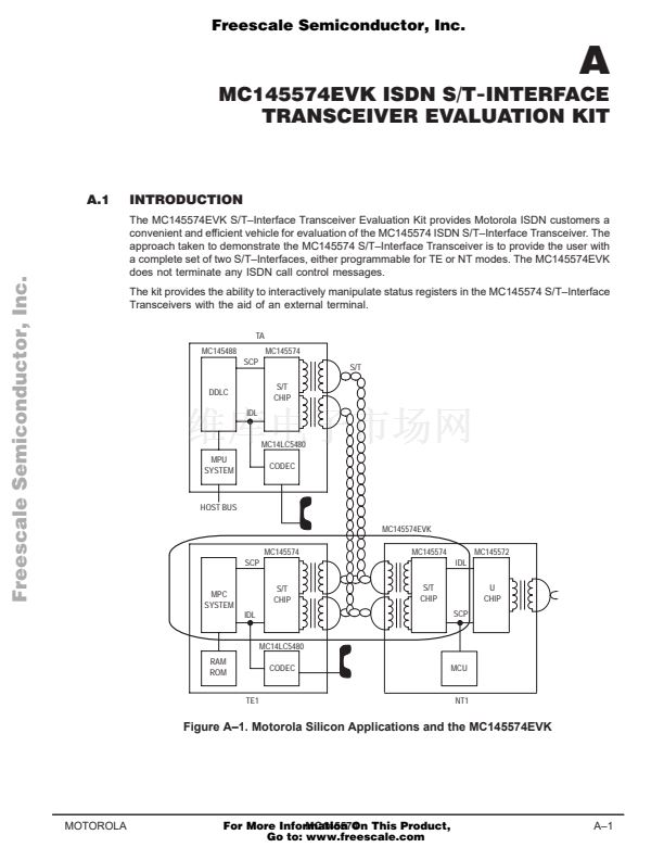
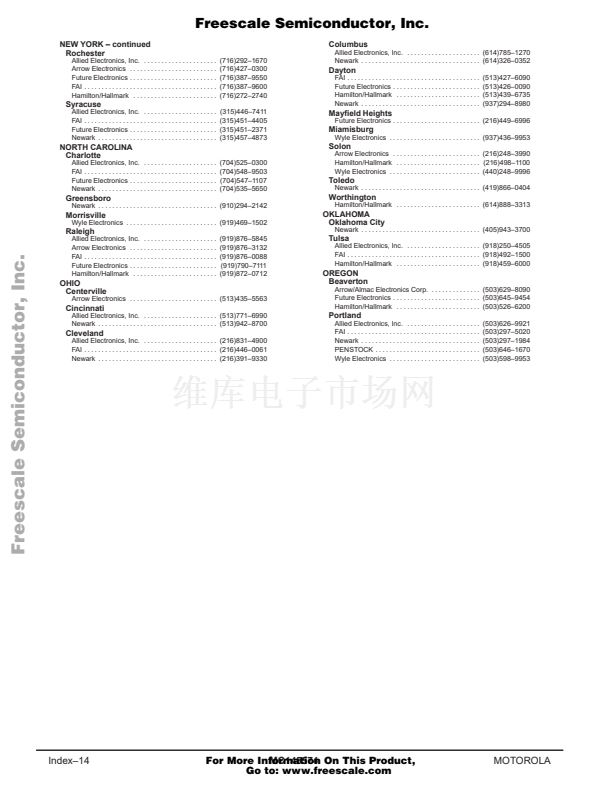
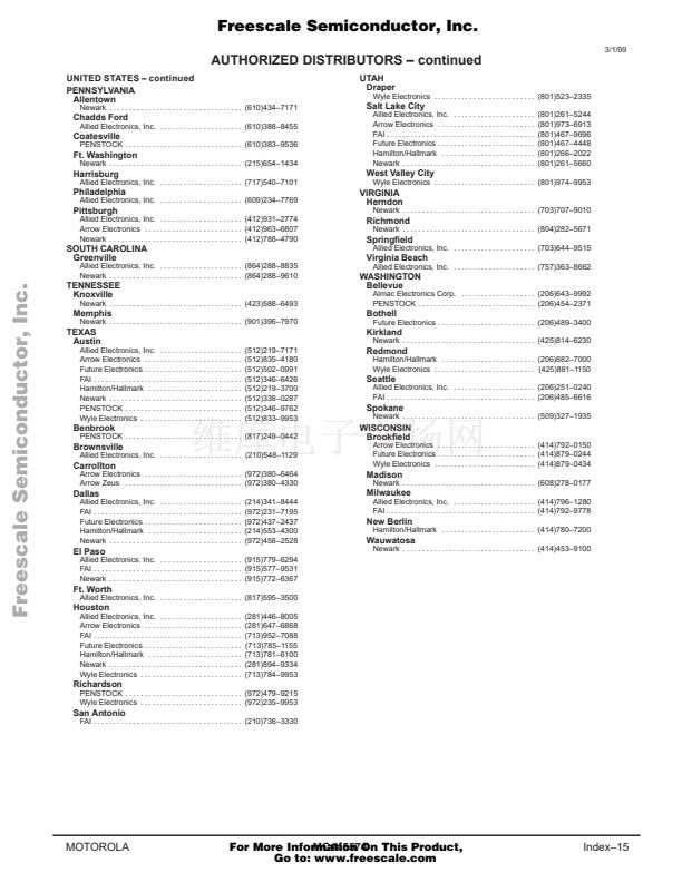
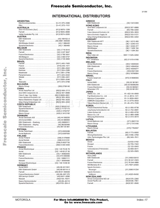
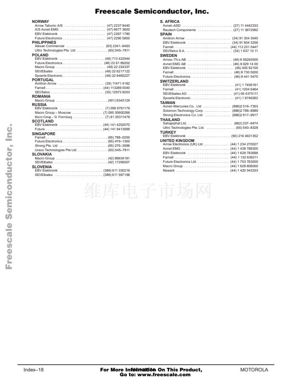
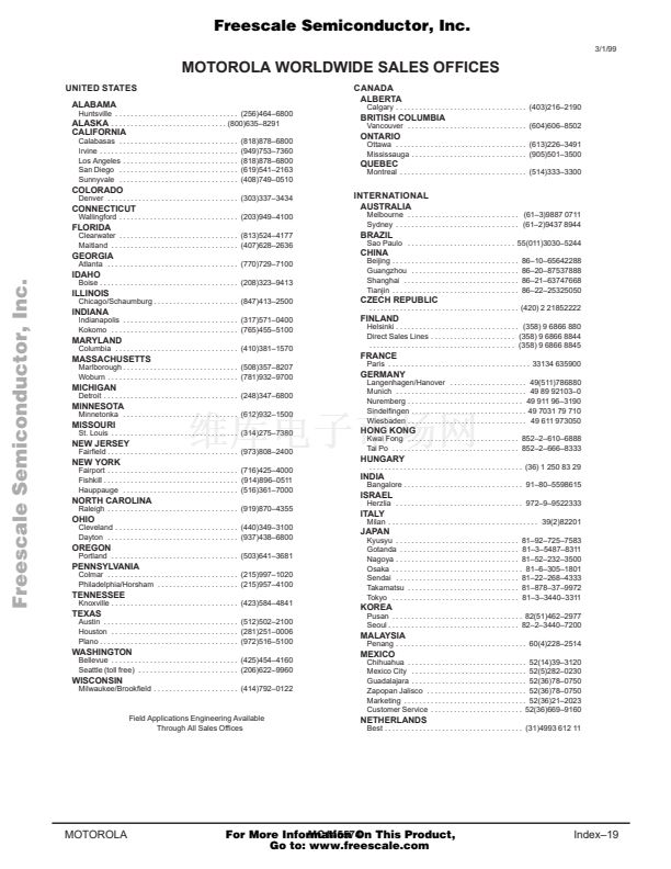
Freescale Semiconductor, Inc.
6.10
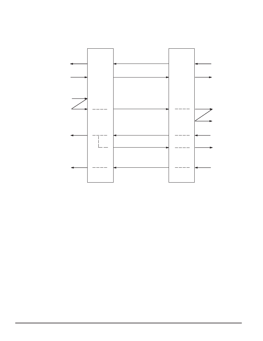
GCI ACTIVATION AND DEACTIVATION TIMING DIAGRAMS
The following diagrams (Figures 6鈥? through 6鈥?) indicate the flow of the activation/deactivation proce-
dure and are not intended to be exhaustive in all the possible permutations.
TEM
NTS
DC
I
Rx
INFO 0
Tx
INFO 0
C
DC
DI
C
Tx
Rx
I
DI
Din = 0
C
C
START
CLOCKS
Tx
INFO 1
Rx
I
Dout = 0 START
CLOCKS
AR
Freescale Semiconductor, Inc...
AR8, AR10
I
INFO 2
AR
I
Rx
Tx
C
AR
Tx
INFO 3
Rx
I
AI
AI8, AI10
I
Rx
INFO 4
Tx
C
AI
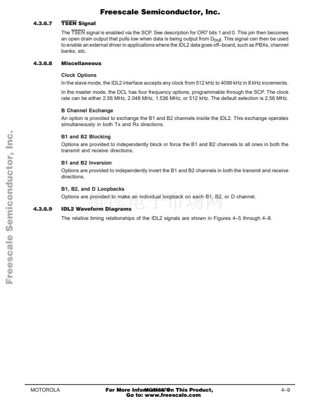
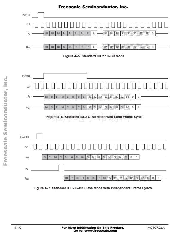
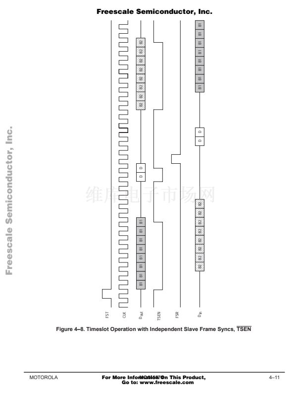
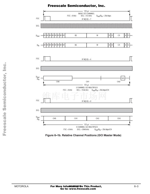
Figure 6鈥?. Activation from TE End
6鈥?4
MC145574
For More Information On This Product,
Go to: www.freescale.com
MOTOROLA


 1
1
 2
2
 3
3
 4
4
 5
5
 6
6
 7
7
 8
8
 9
9
 10
10
 11
11
 12
12
 13
13
 14
14
 15
15
 16
16
 17
17
 18
18
 19
19
 20
20
 21
21
 22
22
 23
23
 24
24
 25
25
 26
26
 27
27
 28
28
 29
29
 30
30
 31
31
 32
32
 33
33
 34
34
 35
35
 36
36
 37
37
 38
38
 39
39
 40
40
 41
41
 42
42
 43
43
 44
44
 45
45
 46
46
 47
47
 48
48
 49
49
 50
50
 51
51
 52
52
 53
53
 54
54
 55
55
 56
56
 57
57
 58
58
 59
59
 60
60
 61
61
 62
62
 63
63
 64
64
 65
65
 66
66
 67
67
 68
68
 69
69
 70
70
 71
71
 72
72
 73
73
 74
74
 75
75
 76
76
 77
77
 78
78
 79
79
 80
80
 81
81
 82
82
 83
83
 84
84
 85
85
 86
86
 87
87
 88
88
 89
89
 90
90
 91
91
 92
92
 93
93
 94
94
 95
95
 96
96
 97
97
 98
98
 99
99
 100
100
 101
101
 102
102
 103
103
 104
104
 105
105
 106
106
 107
107
 108
108
 109
109
 110
110
 111
111
 112
112
 113
113
 114
114
 115
115
 116
116
 117
117
 118
118
 119
119
 120
120
 121
121
 122
122
 123
123
 124
124
 125
125
 126
126
 127
127
 128
128
 129
129
 130
130
 131
131
 132
132
 133
133
 134
134
 135
135
 136
136
 137
137
 138
138
 139
139
 140
140
 141
141
 142
142
 143
143
 144
144
 145
145
 146
146
 147
147
 148
148
 149
149
 150
150
 151
151
 152
152
 153
153
 154
154
 155
155
 156
156
 157
157
 158
158
 159
159
 160
160
 161
161
 162
162
 163
163
 164
164
