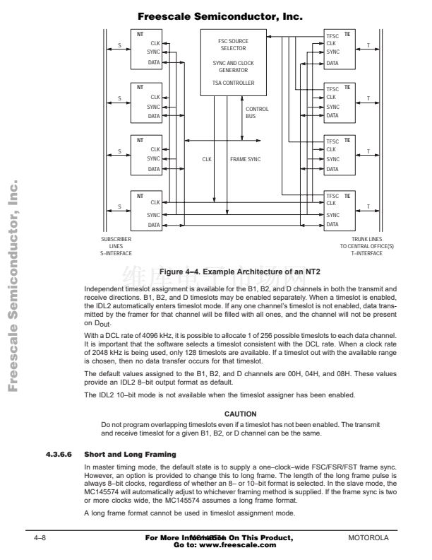
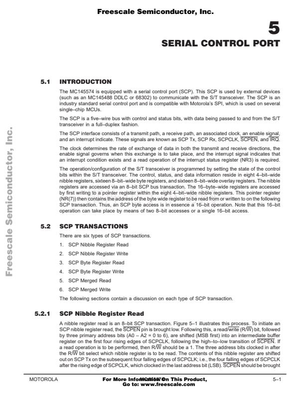
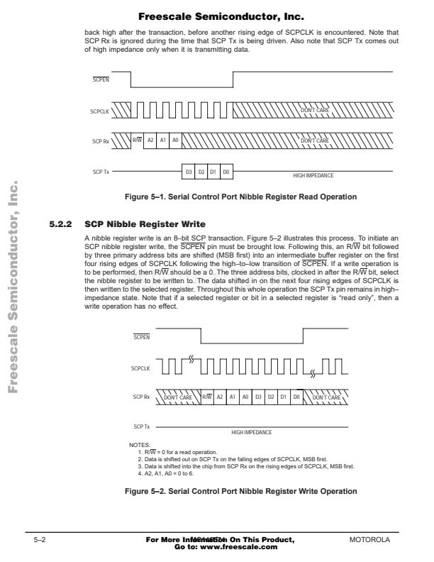
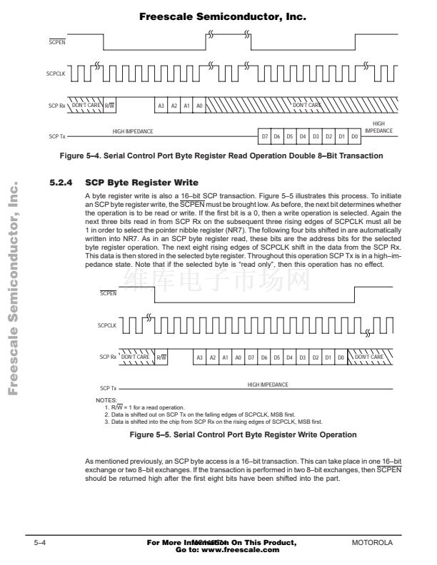
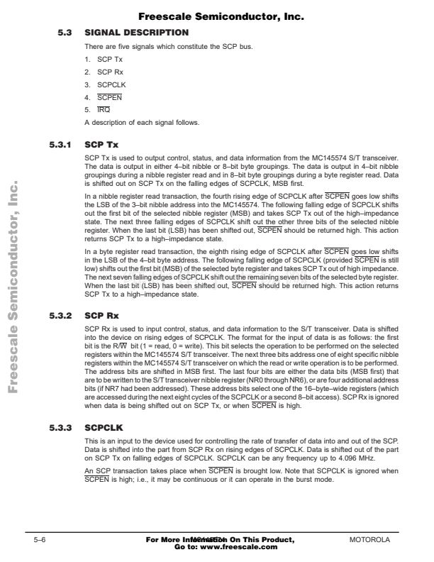
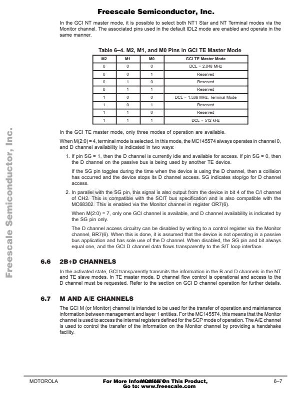
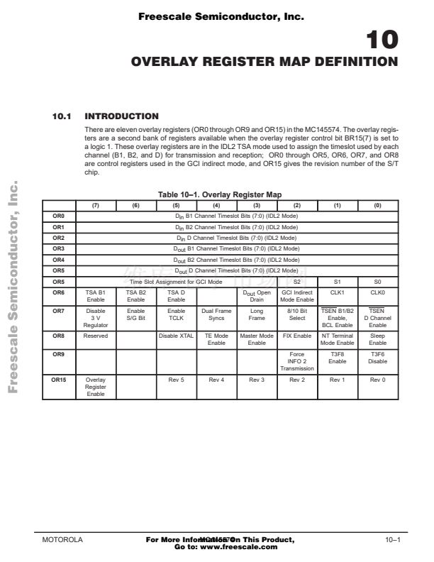
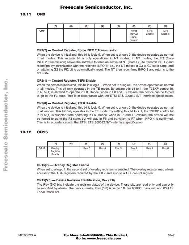
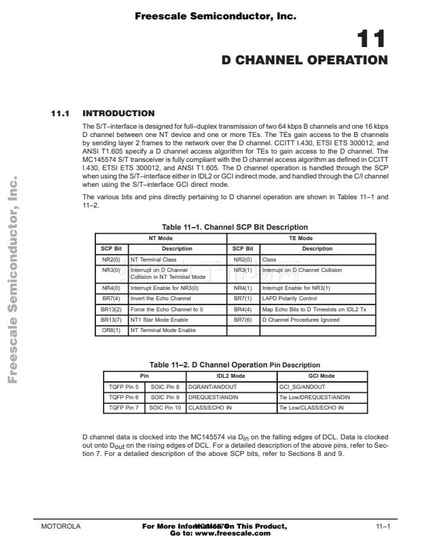
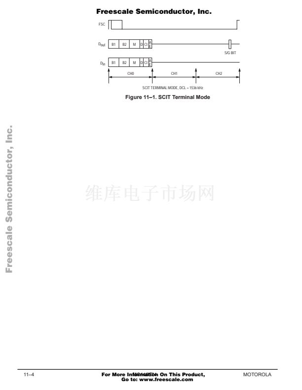
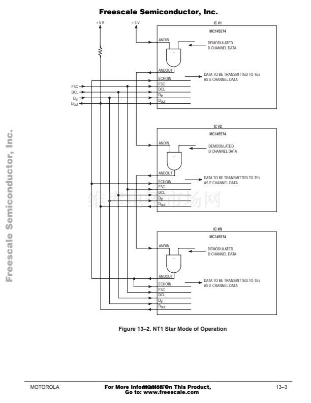
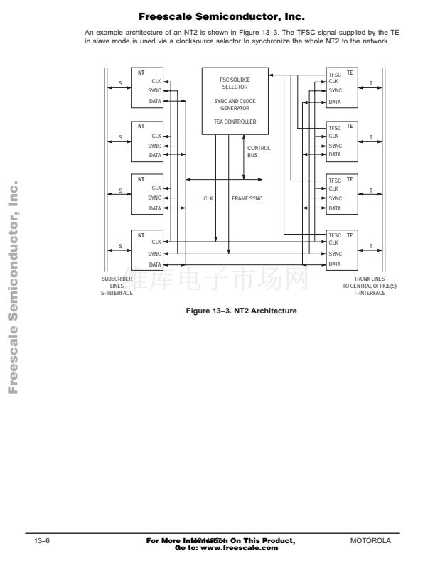
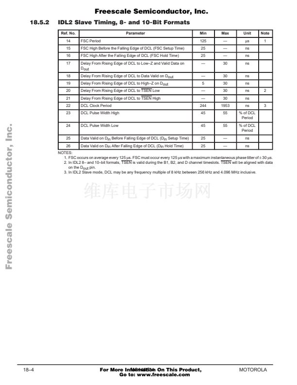
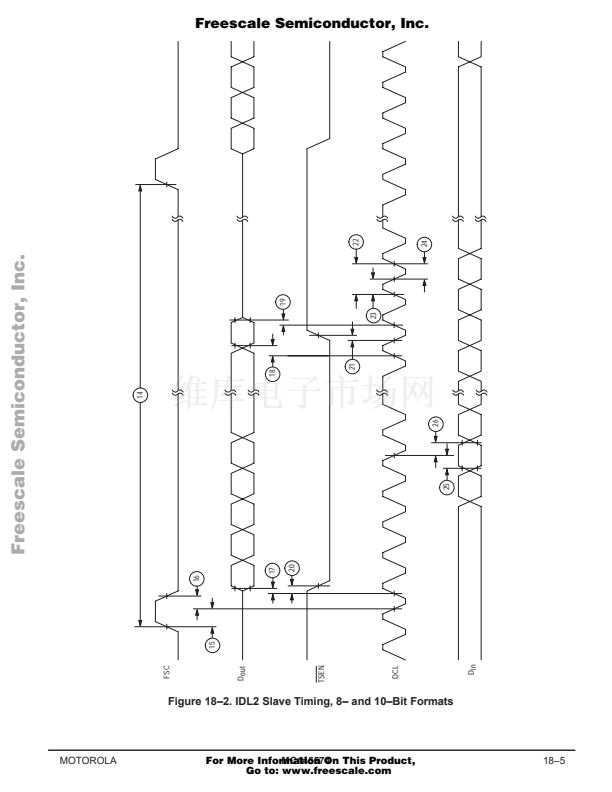
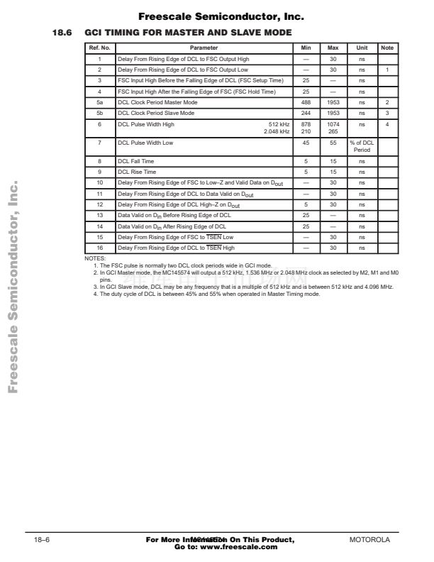
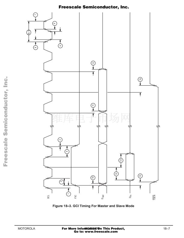
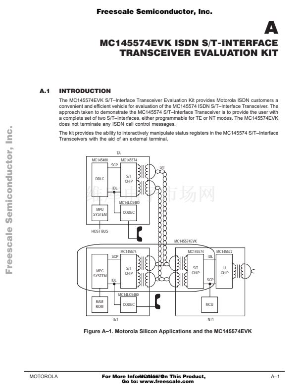
Freescale Semiconductor, Inc.
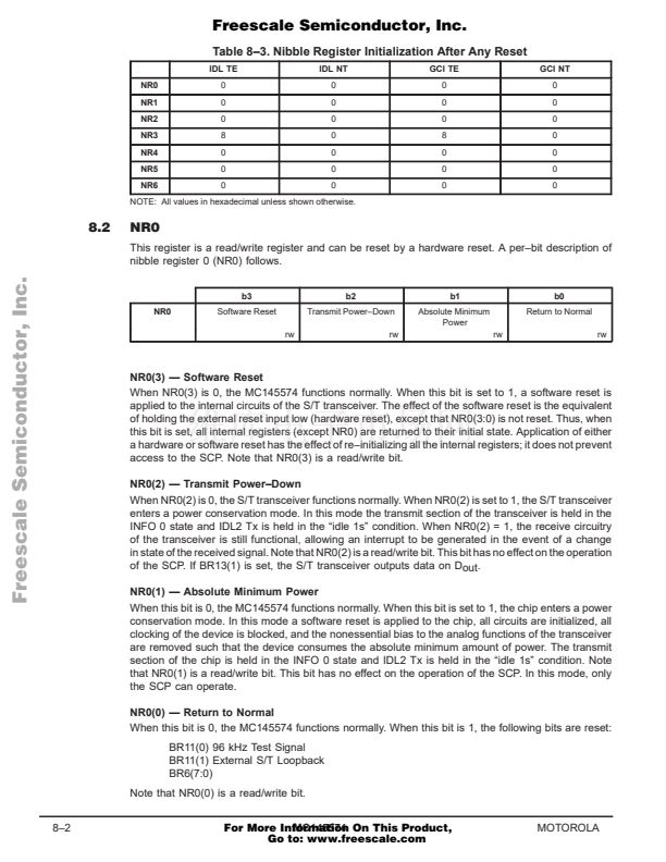
Table 8鈥?. Nibble Register Initialization After Any Reset
IDL TE
NR0
NR1
NR2
NR3
NR4
NR5
NR6
0
0
0
8
0
0
0
IDL NT
0
0
0
0
0
0
0
GCI TE
0
0
0
8
0
0
0
GCI NT
0
0
0
0
0
0
0
NOTE: All values in hexadecimal unless shown otherwise.
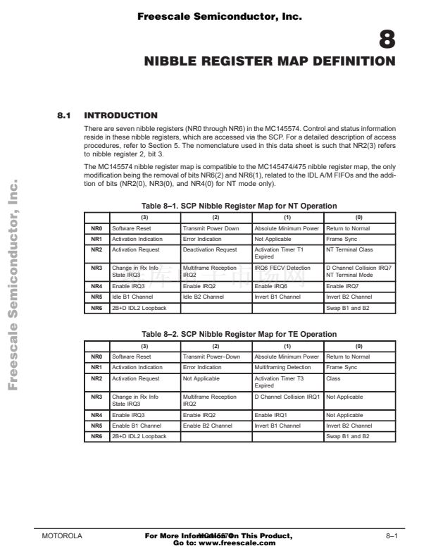
8.2
NR0
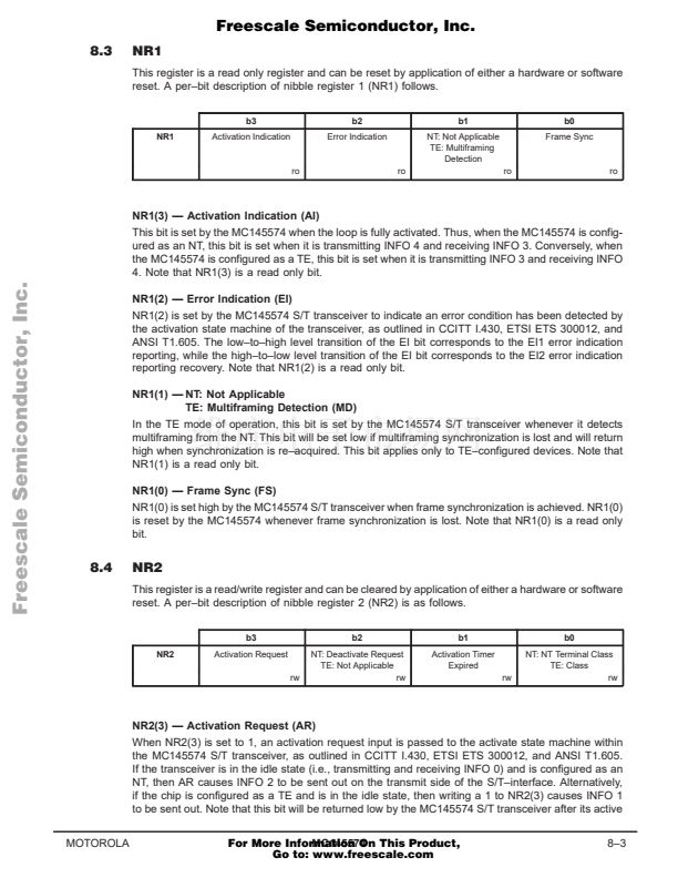
This register is a read/write register and can be reset by a hardware reset. A per鈥揵it description of
nibble register 0 (NR0) follows.
b3
NR0
Software Reset
rw
b2
Transmit Power鈥揇own
rw
b1
Absolute Minimum
Power
rw
b0
Return to Normal
rw
Freescale Semiconductor, Inc...
NR0(3) 鈥?Software Reset
When NR0(3) is 0, the MC145574 functions normally. When this bit is set to 1, a software reset is
applied to the internal circuits of the S/T transceiver. The effect of the software reset is the equivalent
of holding the external reset input low (hardware reset), except that NR0(3:0) is not reset. Thus, when
this bit is set, all internal registers (except NR0) are returned to their initial state. Application of either
a hardware or software reset has the effect of re鈥搃nitializing all the internal registers; it does not prevent
access to the SCP. Note that NR0(3) is a read/write bit.
NR0(2) 鈥?Transmit Power鈥揇own
When NR0(2) is 0, the S/T transceiver functions normally. When NR0(2) is set to 1, the S/T transceiver
enters a power conservation mode. In this mode the transmit section of the transceiver is held in the
INFO 0 state and IDL2 Tx is held in the 鈥渋dle 1s鈥?condition. When NR0(2) = 1, the receive circuitry
of the transceiver is still functional, allowing an interrupt to be generated in the event of a change
in state of the received signal. Note that NR0(2) is a read/write bit. This bit has no effect on the operation
of the SCP. If BR13(1) is set, the S/T transceiver outputs data on Dout.
NR0(1) 鈥?Absolute Minimum Power
When this bit is 0, the MC145574 functions normally. When this bit is set to 1, the chip enters a power
conservation mode. In this mode a software reset is applied to the chip, all circuits are initialized, all
clocking of the device is blocked, and the nonessential bias to the analog functions of the transceiver
are removed such that the device consumes the absolute minimum amount of power. The transmit
section of the chip is held in the INFO 0 state and IDL2 Tx is held in the 鈥渋dle 1s鈥?condition. Note
that NR0(1) is a read/write bit. This bit has no effect on the operation of the SCP. In this mode, only
the SCP can operate.
NR0(0) 鈥?Return to Normal
When this bit is 0, the MC145574 functions normally. When this bit is 1, the following bits are reset:
BR11(0) 96 kHz Test Signal
BR11(1) External S/T Loopback
BR6(7:0)
Note that NR0(0) is a read/write bit.
8鈥?
MC145574
For More Information On This Product,
Go to: www.freescale.com
MOTOROLA


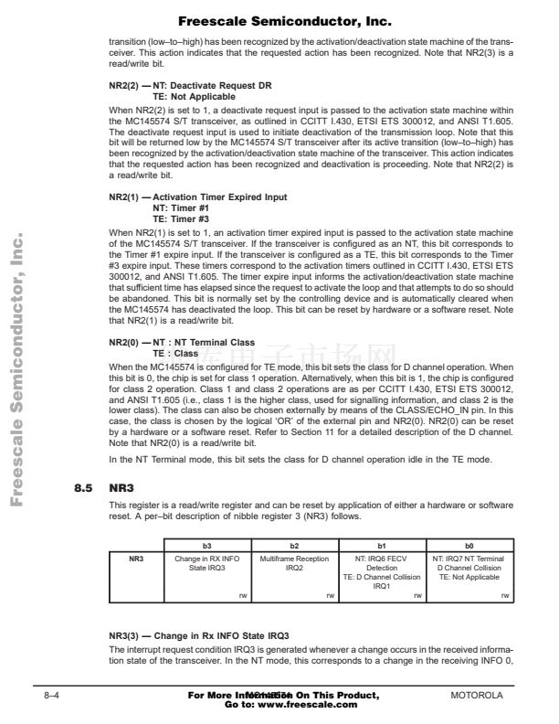
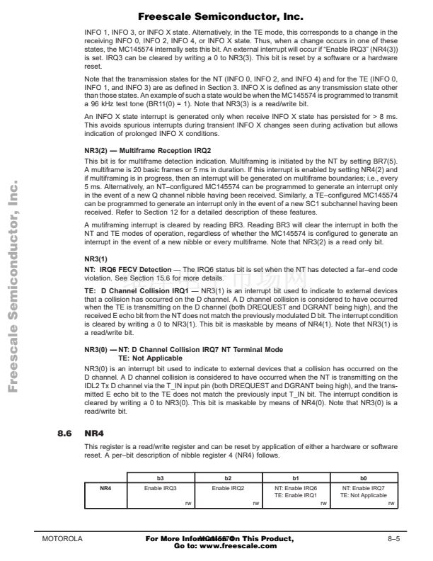
 1
1
 2
2
 3
3
 4
4
 5
5
 6
6
 7
7
 8
8
 9
9
 10
10
 11
11
 12
12
 13
13
 14
14
 15
15
 16
16
 17
17
 18
18
 19
19
 20
20
 21
21
 22
22
 23
23
 24
24
 25
25
 26
26
 27
27
 28
28
 29
29
 30
30
 31
31
 32
32
 33
33
 34
34
 35
35
 36
36
 37
37
 38
38
 39
39
 40
40
 41
41
 42
42
 43
43
 44
44
 45
45
 46
46
 47
47
 48
48
 49
49
 50
50
 51
51
 52
52
 53
53
 54
54
 55
55
 56
56
 57
57
 58
58
 59
59
 60
60
 61
61
 62
62
 63
63
 64
64
 65
65
 66
66
 67
67
 68
68
 69
69
 70
70
 71
71
 72
72
 73
73
 74
74
 75
75
 76
76
 77
77
 78
78
 79
79
 80
80
 81
81
 82
82
 83
83
 84
84
 85
85
 86
86
 87
87
 88
88
 89
89
 90
90
 91
91
 92
92
 93
93
 94
94
 95
95
 96
96
 97
97
 98
98
 99
99
 100
100
 101
101
 102
102
 103
103
 104
104
 105
105
 106
106
 107
107
 108
108
 109
109
 110
110
 111
111
 112
112
 113
113
 114
114
 115
115
 116
116
 117
117
 118
118
 119
119
 120
120
 121
121
 122
122
 123
123
 124
124
 125
125
 126
126
 127
127
 128
128
 129
129
 130
130
 131
131
 132
132
 133
133
 134
134
 135
135
 136
136
 137
137
 138
138
 139
139
 140
140
 141
141
 142
142
 143
143
 144
144
 145
145
 146
146
 147
147
 148
148
 149
149
 150
150
 151
151
 152
152
 153
153
 154
154
 155
155
 156
156
 157
157
 158
158
 159
159
 160
160
 161
161
 162
162
 163
163
 164
164
