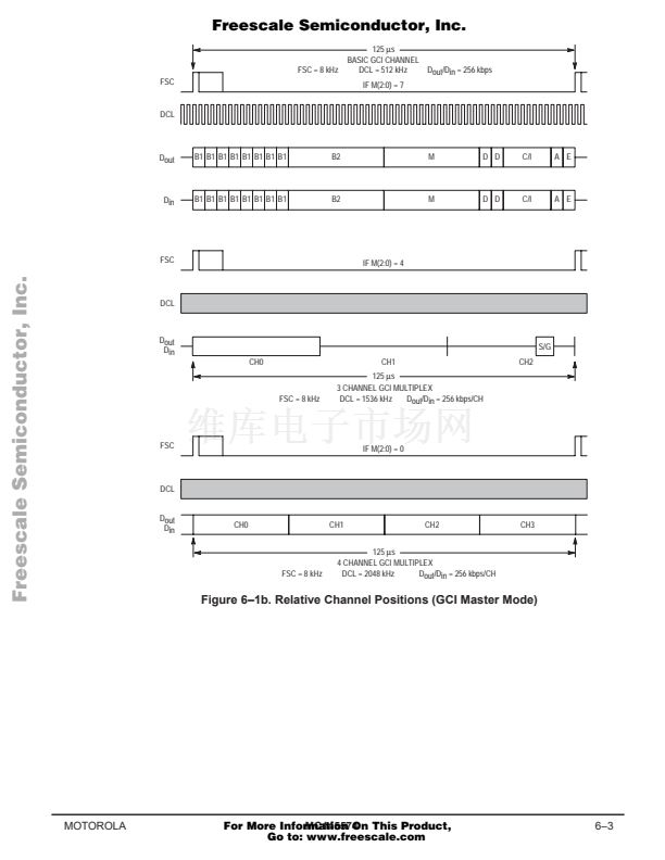
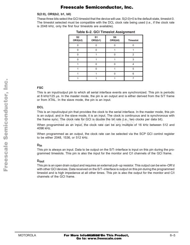
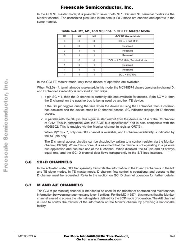
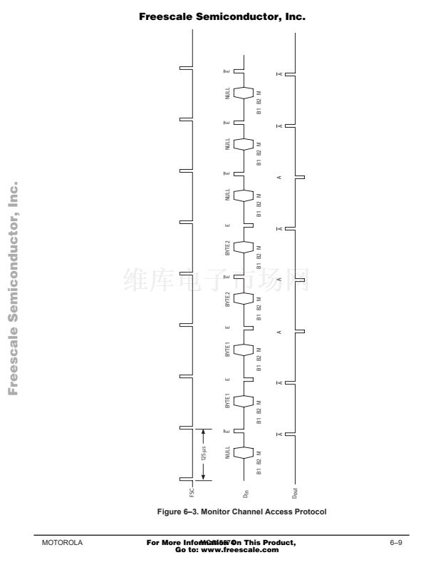
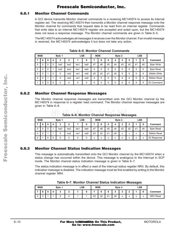
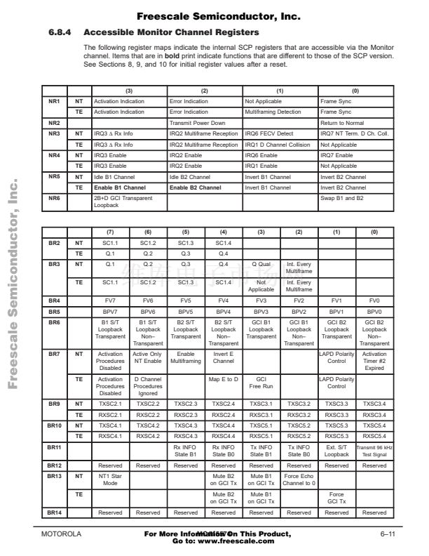
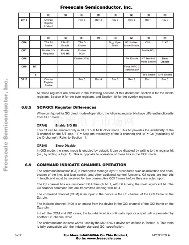
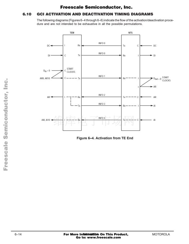
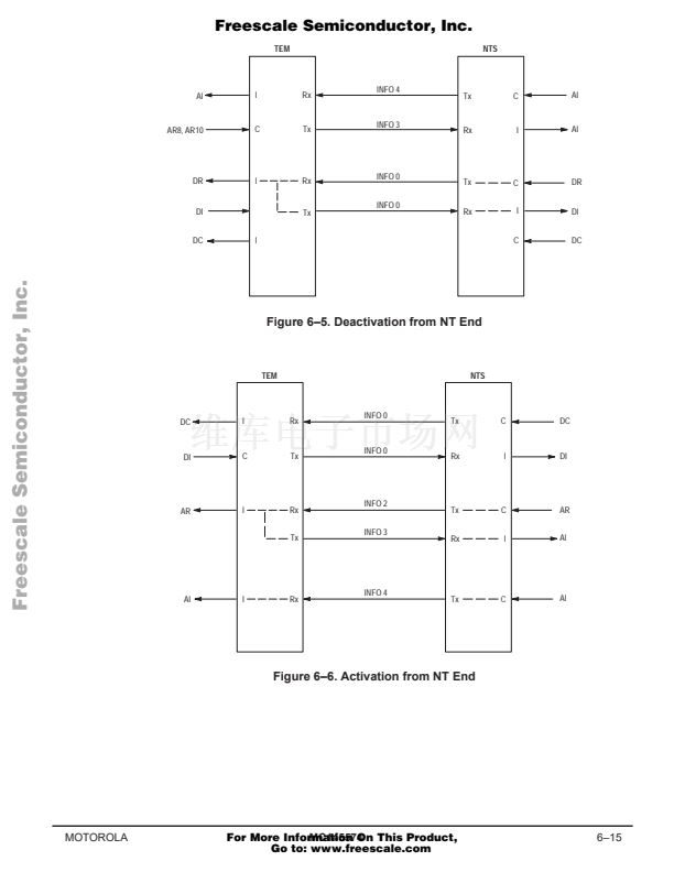
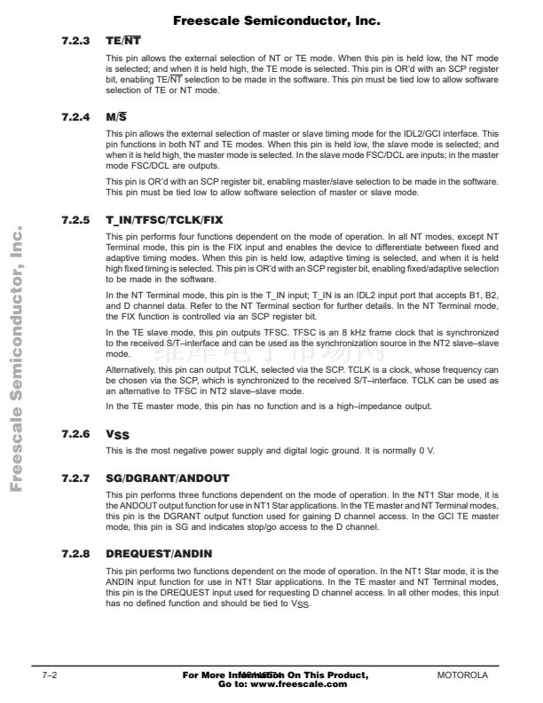
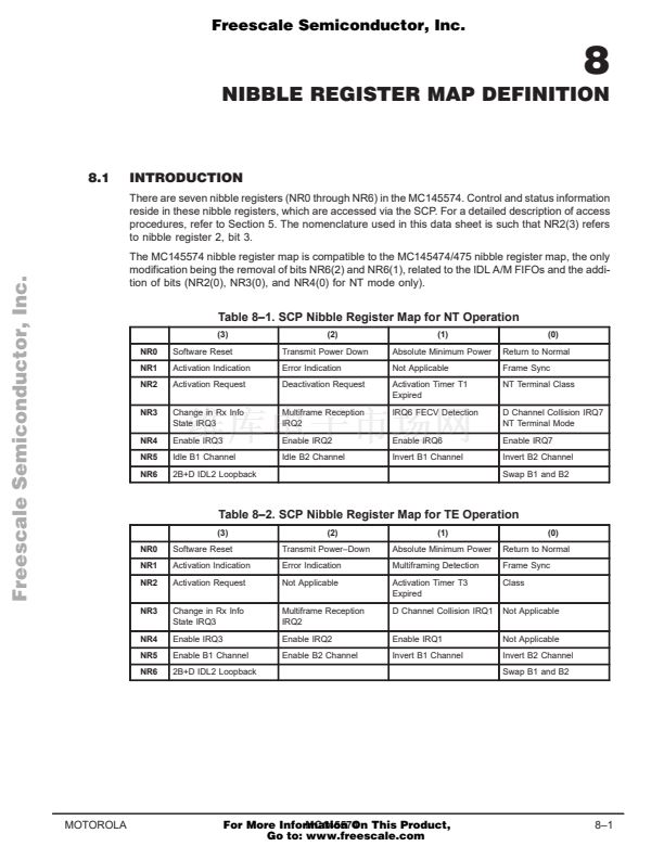
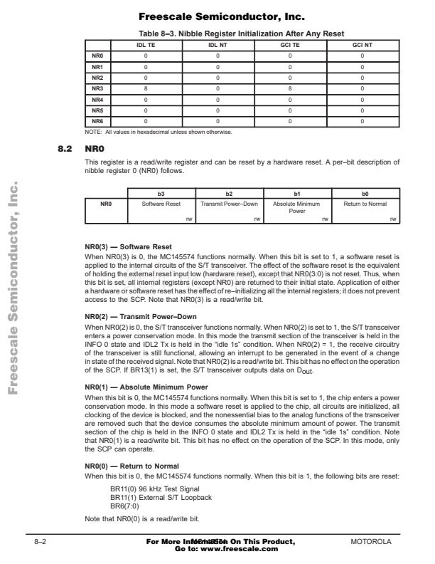
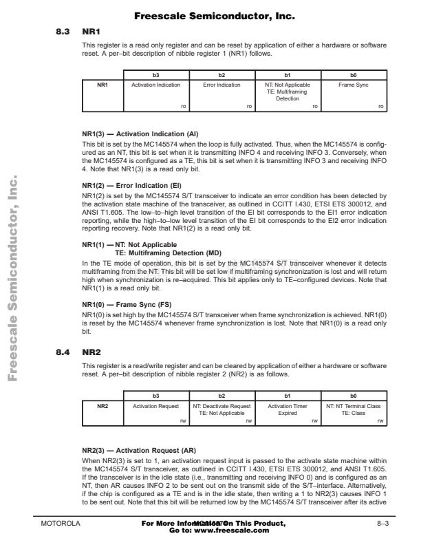
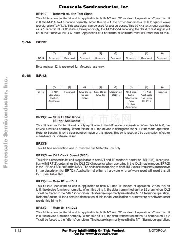
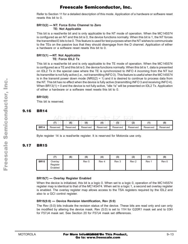
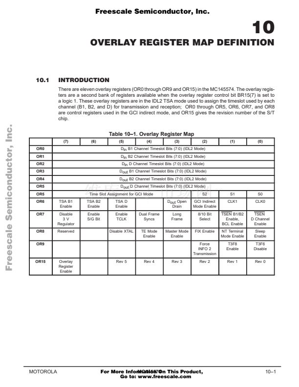
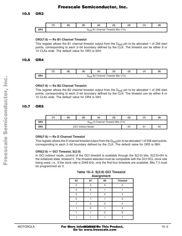
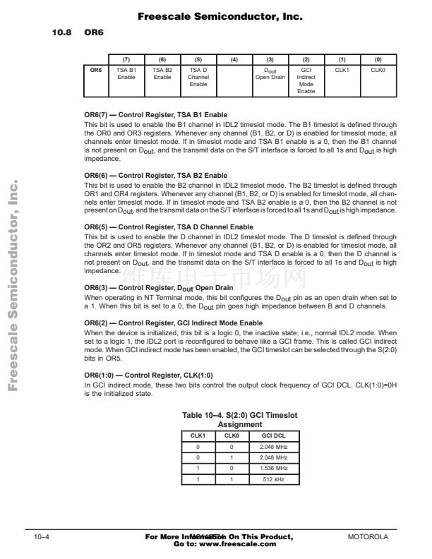
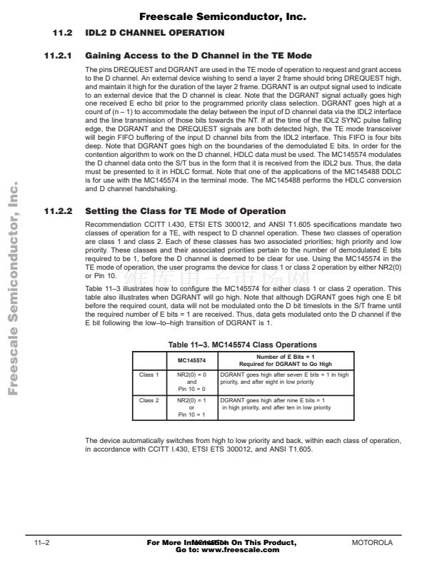
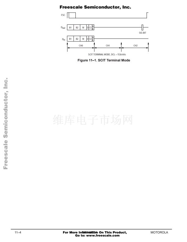
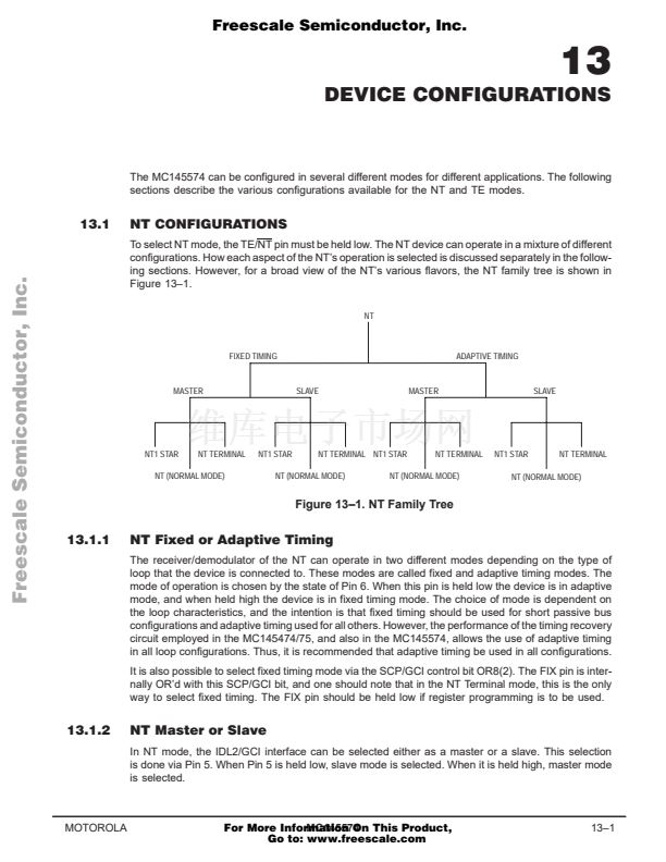
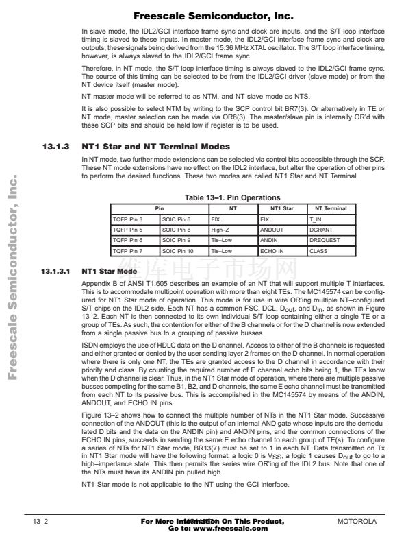
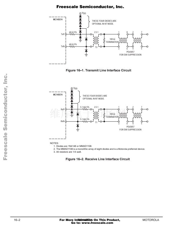
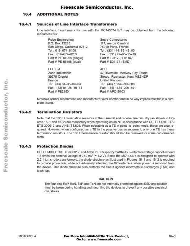
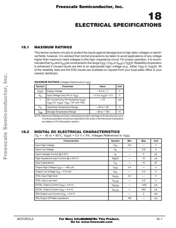
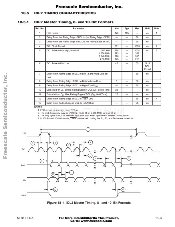
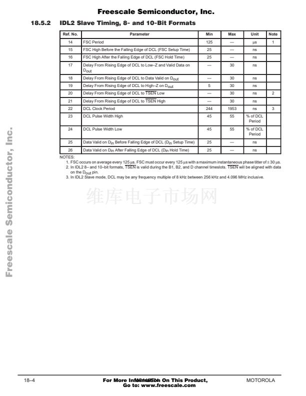
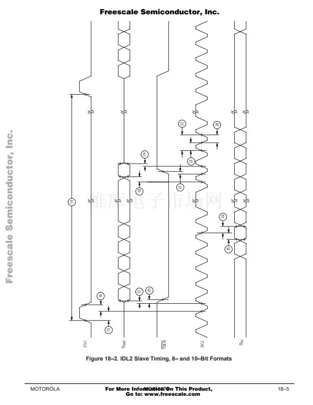
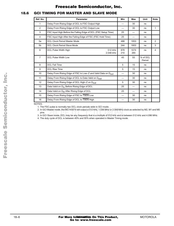
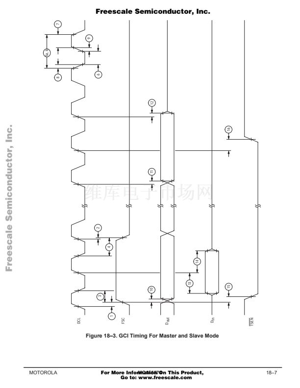
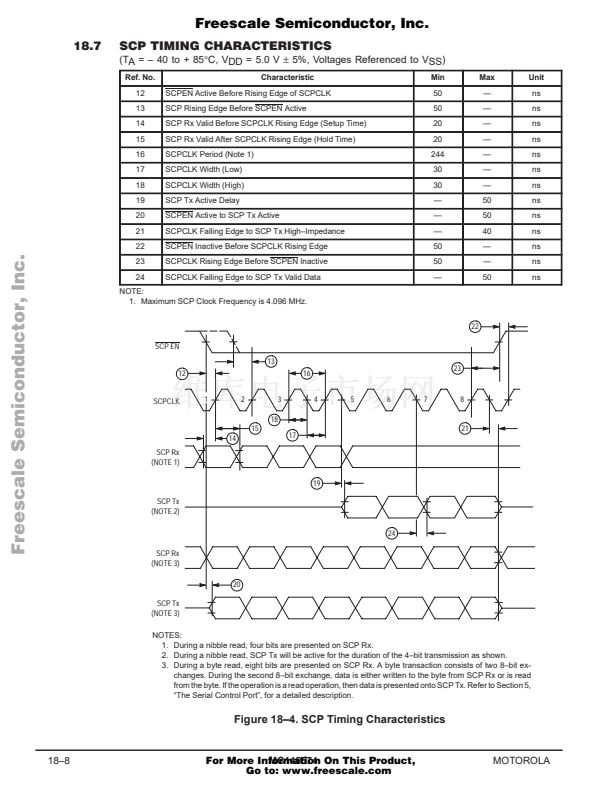
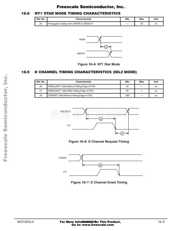
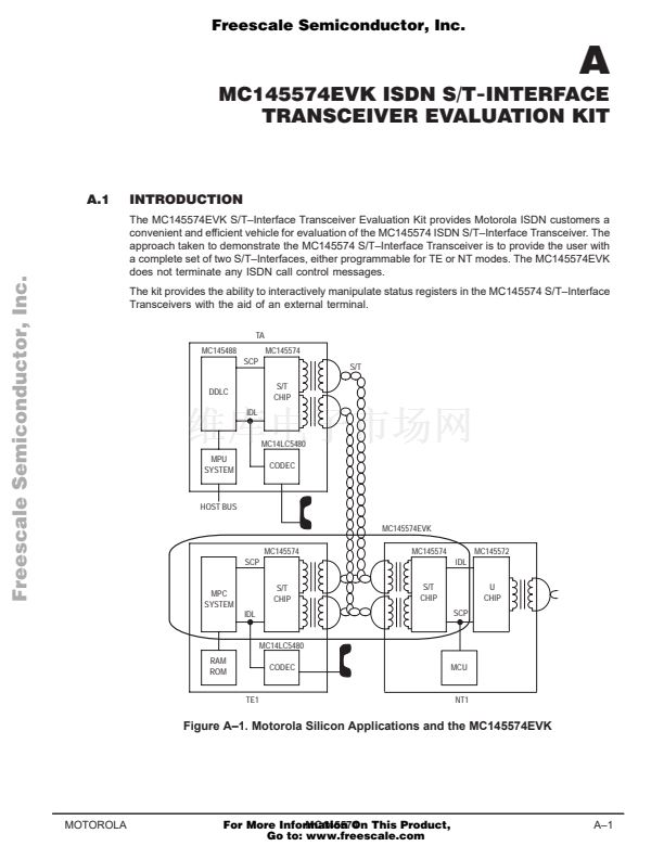
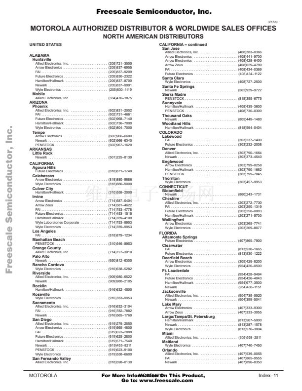
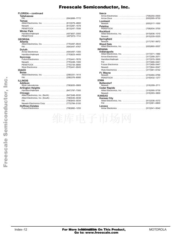
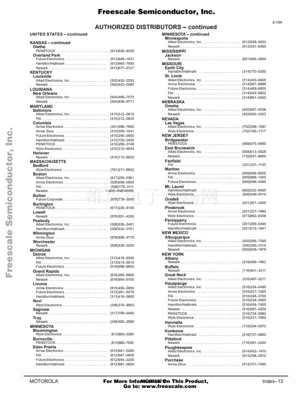
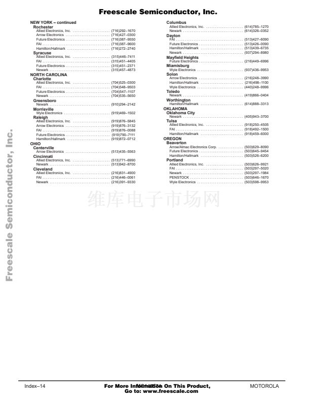
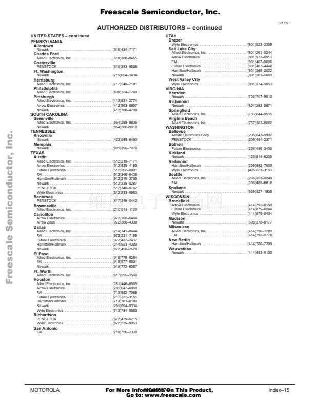
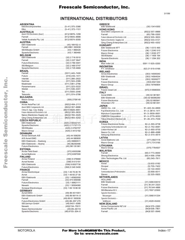
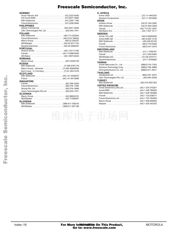
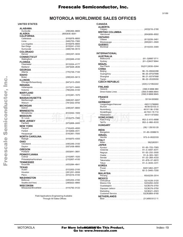
Freescale Semiconductor, Inc.
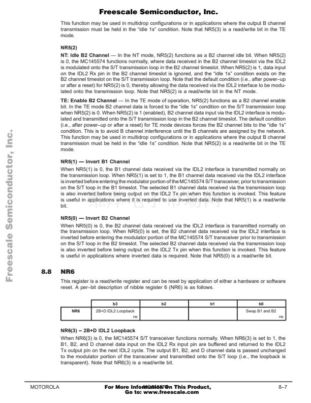
NR6(0) 鈥?Swap B1 and B2
When NR6(0) is 0, the timeslot assigned positions of the B1 and B2 channel data input and output
via the IDL2 interface functions normally. When NR6(0) is set to 1, the timeslot positions of the B1
and B2 channels are reversed; i.e., data entering the device on IDL2 Rx in the B1 timeslot is modulated
onto the B2 timeslot, on the S/T loop. Data demodulated from the B2 timeslot from the S/T loop is
output on IDL2 Tx in the B1 timeslot. The situation is analogous for B2 data entering the device on
IDL2 Rx. This feature is useful in applications where a particular device (such as a codec filter) is
hard鈥搘ired to a particular IDL2 timeslot and needs to gain access to the opposite B channel timeslot.
NR6(0) has no effect during a 2B+D IDL2 loopback. Note that NR6(0) is a read/write bit.
NOTE: When NR6(0) is set, the B channel used on the IDL bus must be enabled before being output
on the S/T loop. For example, if data entering the device on Din in the B1 channel is modulated onto
the B2 channel on the S/T loop, then NR5(3) has to be set. On the MC145474/75, this is done differently.
For the same example, NR5(2) is set instead of NR5(3).
8.9
NR7
NR7 is a pointer register used when accessing a 16鈥揵yte鈥搘ide register. This pointer register will con-
tain the address of the byte鈥搘ide register to be read from or written to, on the following SCP transaction.
This nibble register is not shown on the register map, as it is not programmable.
Freescale Semiconductor, Inc...
8鈥?
MC145574
For More Information On This Product,
Go to: www.freescale.com
MOTOROLA


 1
1
 2
2
 3
3
 4
4
 5
5
 6
6
 7
7
 8
8
 9
9
 10
10
 11
11
 12
12
 13
13
 14
14
 15
15
 16
16
 17
17
 18
18
 19
19
 20
20
 21
21
 22
22
 23
23
 24
24
 25
25
 26
26
 27
27
 28
28
 29
29
 30
30
 31
31
 32
32
 33
33
 34
34
 35
35
 36
36
 37
37
 38
38
 39
39
 40
40
 41
41
 42
42
 43
43
 44
44
 45
45
 46
46
 47
47
 48
48
 49
49
 50
50
 51
51
 52
52
 53
53
 54
54
 55
55
 56
56
 57
57
 58
58
 59
59
 60
60
 61
61
 62
62
 63
63
 64
64
 65
65
 66
66
 67
67
 68
68
 69
69
 70
70
 71
71
 72
72
 73
73
 74
74
 75
75
 76
76
 77
77
 78
78
 79
79
 80
80
 81
81
 82
82
 83
83
 84
84
 85
85
 86
86
 87
87
 88
88
 89
89
 90
90
 91
91
 92
92
 93
93
 94
94
 95
95
 96
96
 97
97
 98
98
 99
99
 100
100
 101
101
 102
102
 103
103
 104
104
 105
105
 106
106
 107
107
 108
108
 109
109
 110
110
 111
111
 112
112
 113
113
 114
114
 115
115
 116
116
 117
117
 118
118
 119
119
 120
120
 121
121
 122
122
 123
123
 124
124
 125
125
 126
126
 127
127
 128
128
 129
129
 130
130
 131
131
 132
132
 133
133
 134
134
 135
135
 136
136
 137
137
 138
138
 139
139
 140
140
 141
141
 142
142
 143
143
 144
144
 145
145
 146
146
 147
147
 148
148
 149
149
 150
150
 151
151
 152
152
 153
153
 154
154
 155
155
 156
156
 157
157
 158
158
 159
159
 160
160
 161
161
 162
162
 163
163
 164
164
