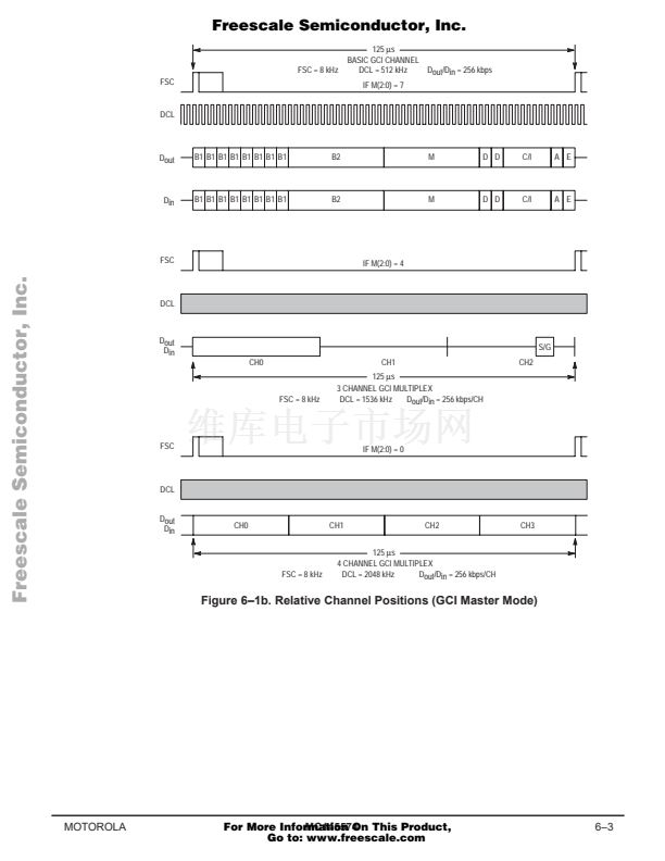
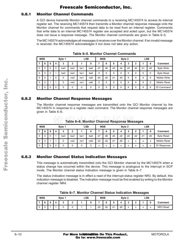
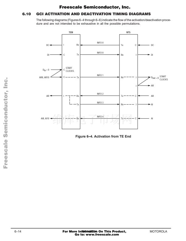
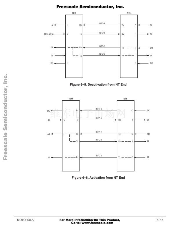
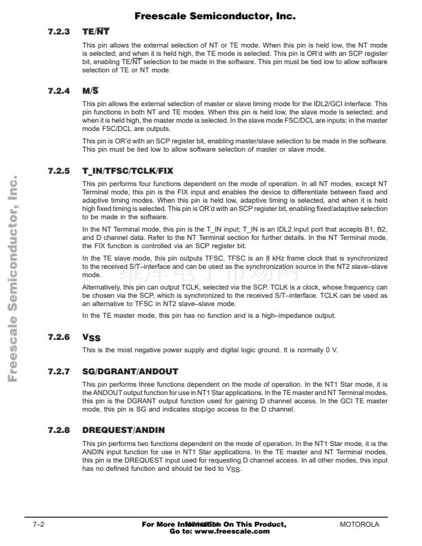
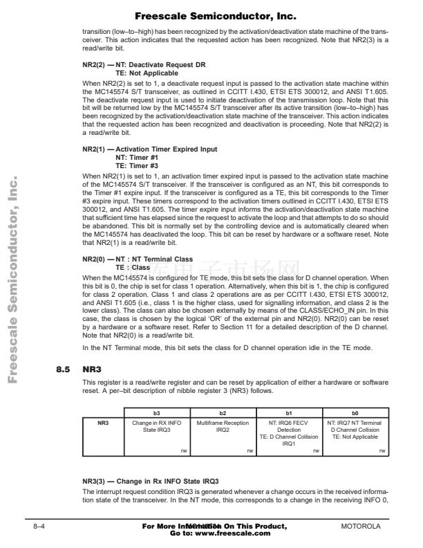
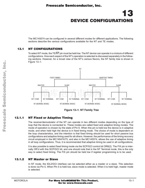
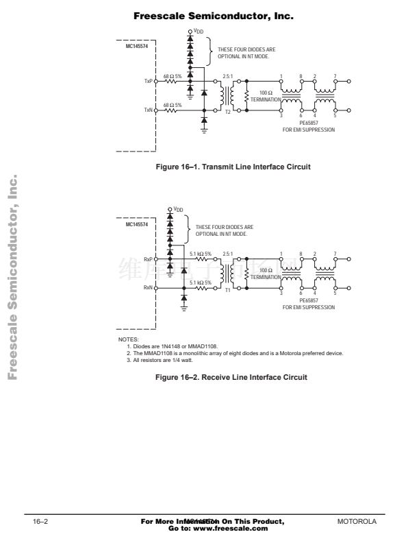
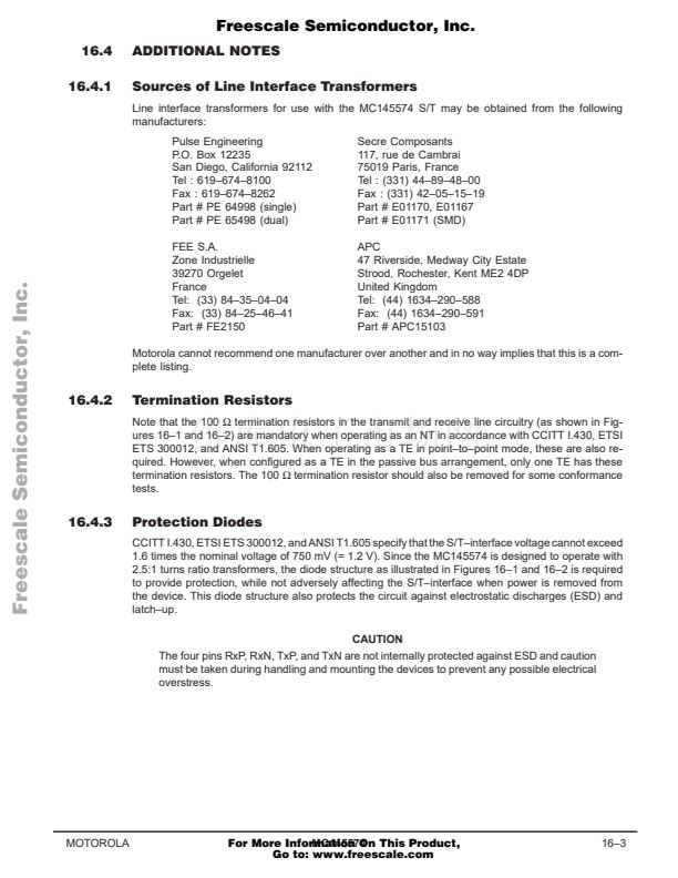
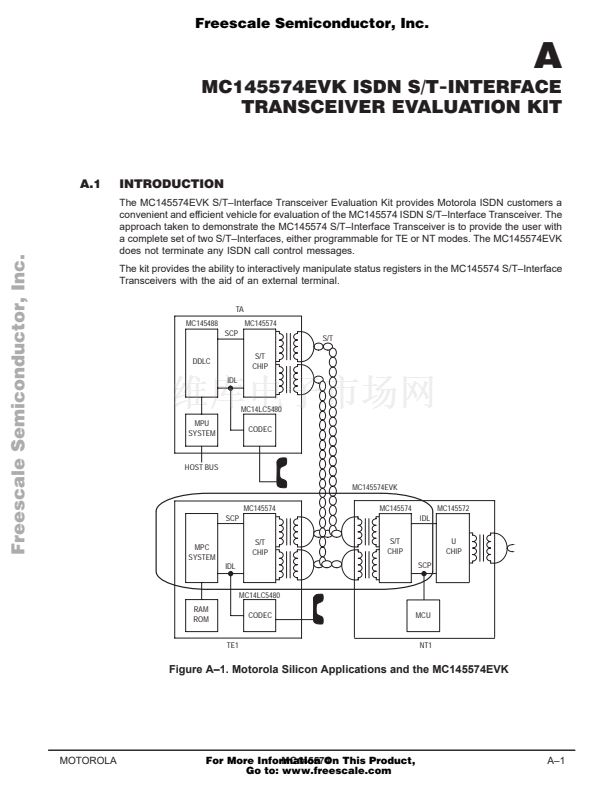
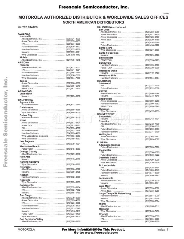
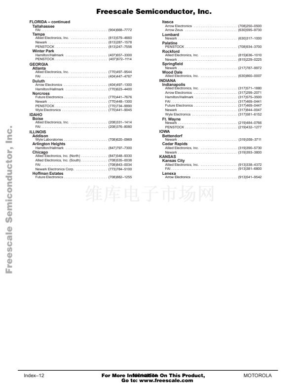
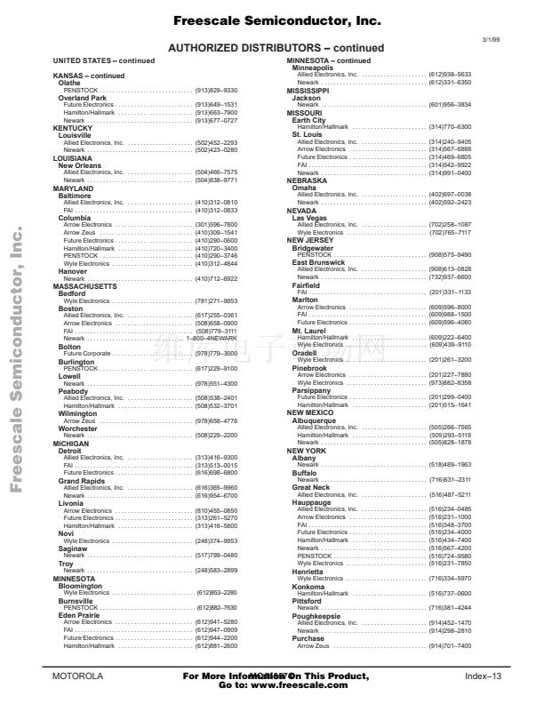
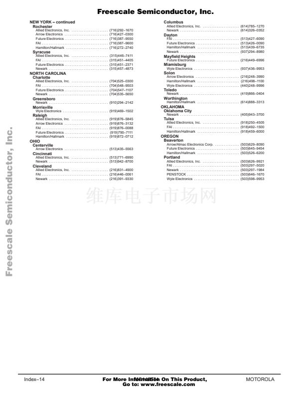
Freescale Semiconductor, Inc.
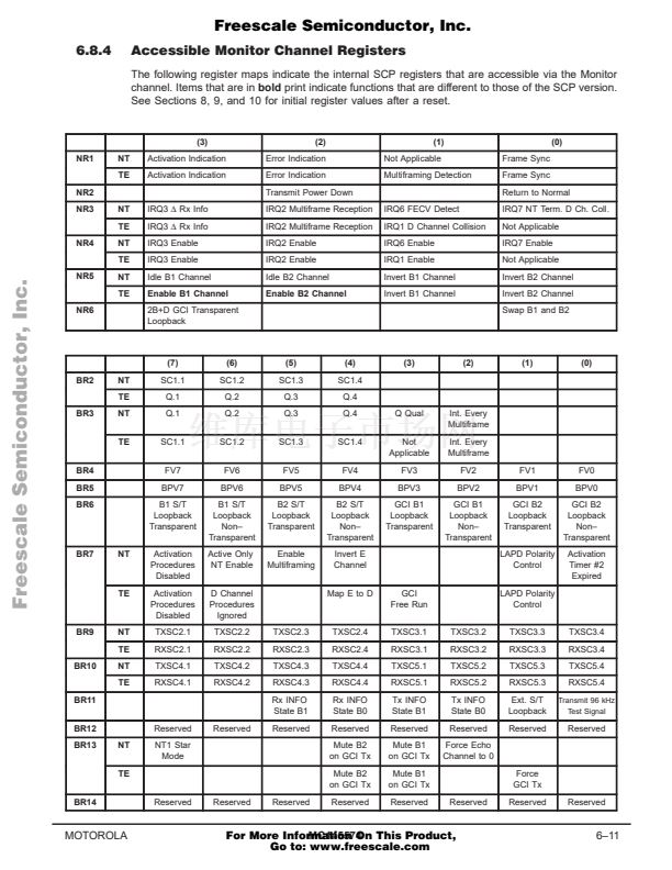
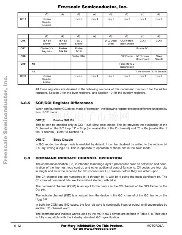
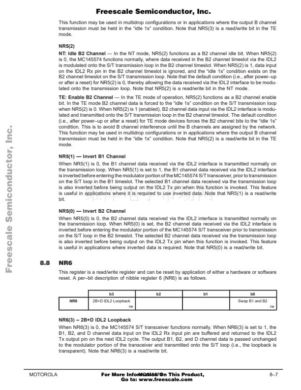
OVERLAY REGISTER MAP DEFINITION
10
10.1
INTRODUCTION
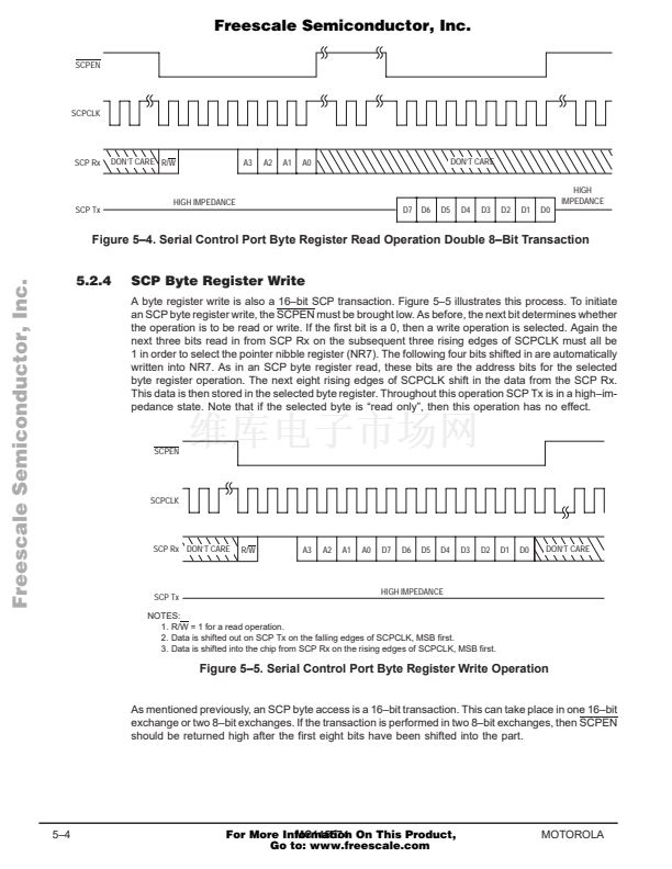
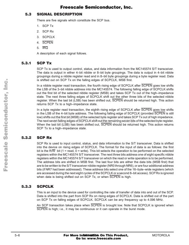
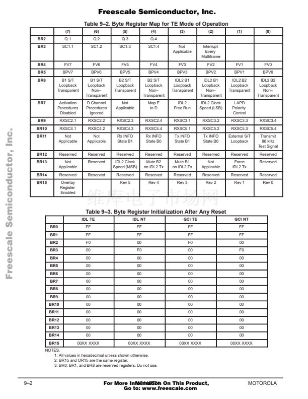
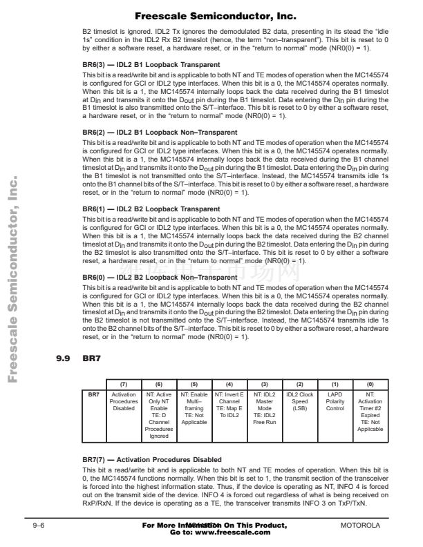
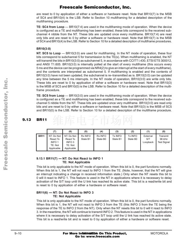
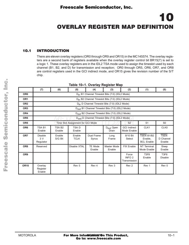
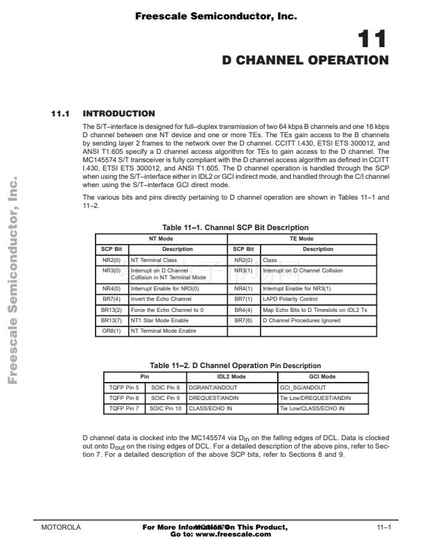
There are eleven overlay registers (OR0 through OR9 and OR15) in the MC145574. The overlay regis-
ters are a second bank of registers available when the overlay register control bit BR15(7) is set to
a logic 1. These overlay registers are in the IDL2 TSA mode used to assign the timeslot used by each
channel (B1, B2, and D) for transmission and reception; OR0 through OR5, OR6, OR7, and OR8
are control registers used in the GCI indirect mode, and OR15 gives the revision number of the S/T
chip.
Freescale Semiconductor, Inc...
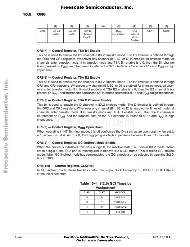
Table 10鈥?. Overlay Register Map
(7)
OR0
OR1
OR2
OR3
OR4
OR5
OR5
OR6
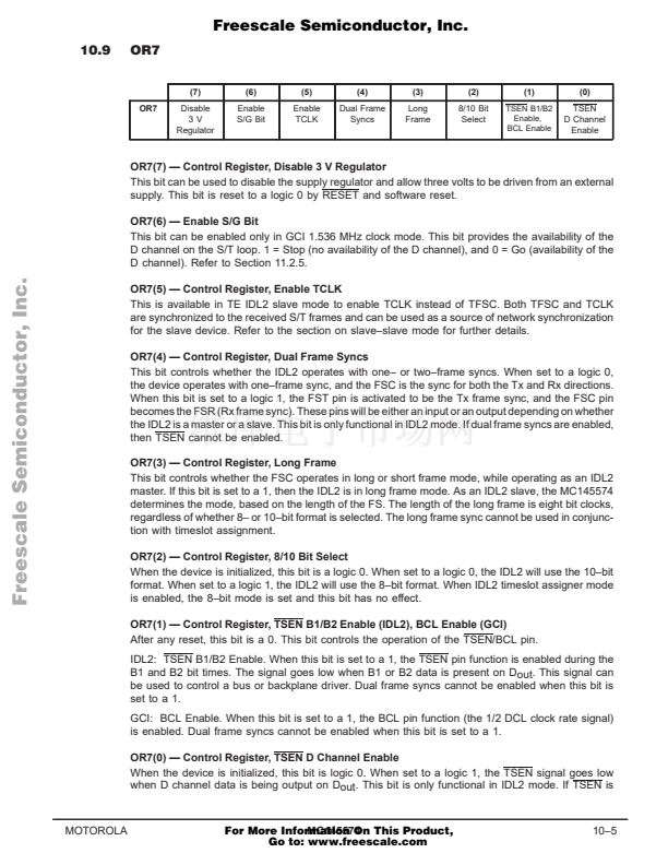
OR7
TSA B1
Enable
Disable
3V
Regulator
Reserved
(6)
(5)
(4)
(3)
(2)
(1)
(0)
Din B1 Channel Timeslot Bits (7:0) (IDL2 Mode)
Din B2 Channel Timeslot Bits (7:0) (IDL2 Mode)
Din D Channel Timeslot Bits (7:0) (IDL2 Mode)
Dout B1 Channel Timeslot Bits (7:0) (IDL2 Mode)
Dout B2 Channel Timeslot Bits (7:0) (IDL2 Mode)
Dout D Channel Timeslot Bits (7:0) (IDL2 Mode)
Time Slot Assignment for GCI Mode
TSA B2
Enable
Enable
S/G Bit
TSA D
Enable
Enable
TCLK
Disable XTAL
Dual Frame
Syncs
TE Mode
Enable
Dout Open
Drain
Long
Frame
Master Mode
Enable
S2
GCI Indirect
Mode Enable
8/10 Bit
Select
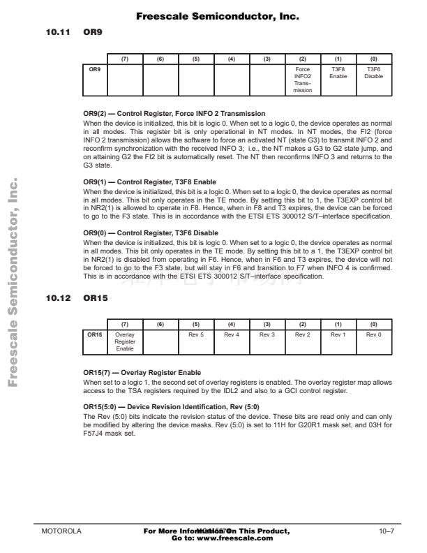
FIX Enable
Force
INFO 2
Transmission
Overlay
Register
Enable
Rev 5
Rev 4
Rev 3
Rev 2
S1
CLK1
TSEN B1/B2
Enable,
BCL Enable
NT Terminal
Mode Enable
T3F8
Enable
Rev 1
S0
CLK0
TSEN
D Channel
Enable
Sleep
Enable
T3F6
Disable
Rev 0
OR8
OR9
OR15
MOTOROLA
MC145574
For More Information On This Product,
Go to: www.freescale.com
10鈥?


 1
1
 2
2
 3
3
 4
4
 5
5
 6
6
 7
7
 8
8
 9
9
 10
10
 11
11
 12
12
 13
13
 14
14
 15
15
 16
16
 17
17
 18
18
 19
19
 20
20
 21
21
 22
22
 23
23
 24
24
 25
25
 26
26
 27
27
 28
28
 29
29
 30
30
 31
31
 32
32
 33
33
 34
34
 35
35
 36
36
 37
37
 38
38
 39
39
 40
40
 41
41
 42
42
 43
43
 44
44
 45
45
 46
46
 47
47
 48
48
 49
49
 50
50
 51
51
 52
52
 53
53
 54
54
 55
55
 56
56
 57
57
 58
58
 59
59
 60
60
 61
61
 62
62
 63
63
 64
64
 65
65
 66
66
 67
67
 68
68
 69
69
 70
70
 71
71
 72
72
 73
73
 74
74
 75
75
 76
76
 77
77
 78
78
 79
79
 80
80
 81
81
 82
82
 83
83
 84
84
 85
85
 86
86
 87
87
 88
88
 89
89
 90
90
 91
91
 92
92
 93
93
 94
94
 95
95
 96
96
 97
97
 98
98
 99
99
 100
100
 101
101
 102
102
 103
103
 104
104
 105
105
 106
106
 107
107
 108
108
 109
109
 110
110
 111
111
 112
112
 113
113
 114
114
 115
115
 116
116
 117
117
 118
118
 119
119
 120
120
 121
121
 122
122
 123
123
 124
124
 125
125
 126
126
 127
127
 128
128
 129
129
 130
130
 131
131
 132
132
 133
133
 134
134
 135
135
 136
136
 137
137
 138
138
 139
139
 140
140
 141
141
 142
142
 143
143
 144
144
 145
145
 146
146
 147
147
 148
148
 149
149
 150
150
 151
151
 152
152
 153
153
 154
154
 155
155
 156
156
 157
157
 158
158
 159
159
 160
160
 161
161
 162
162
 163
163
 164
164
