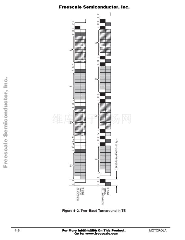
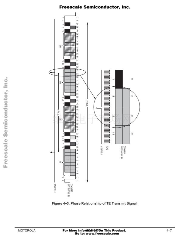
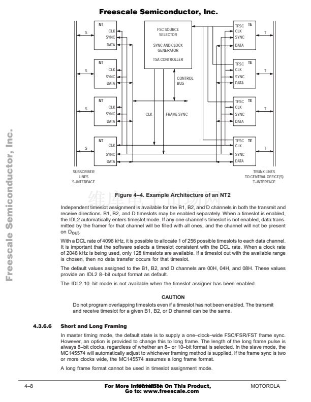
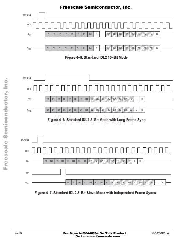
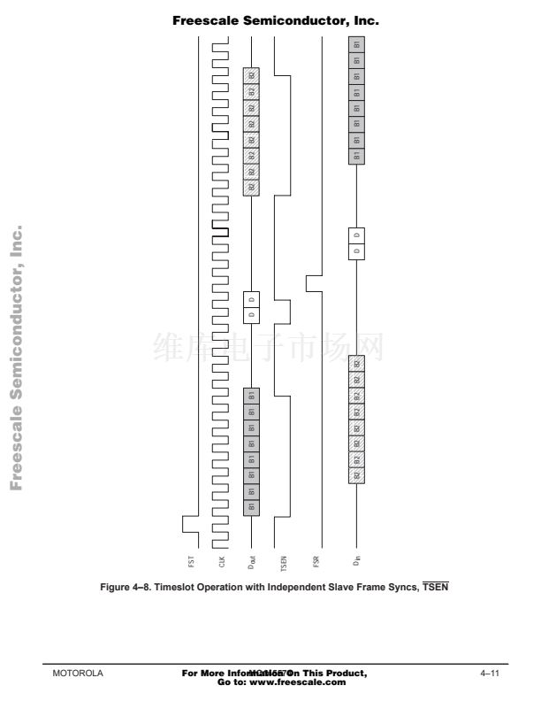
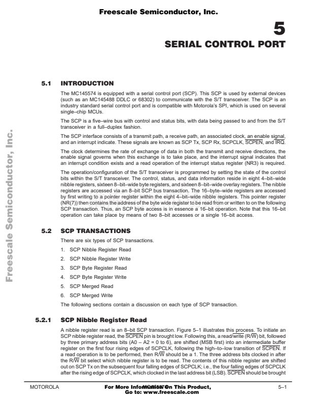
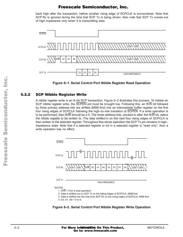
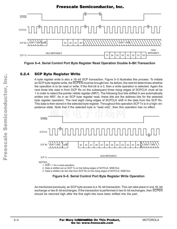
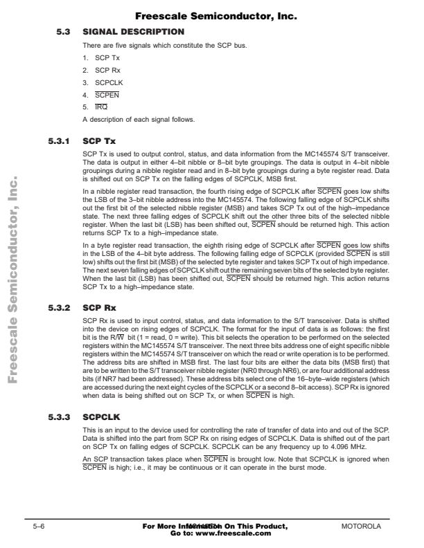
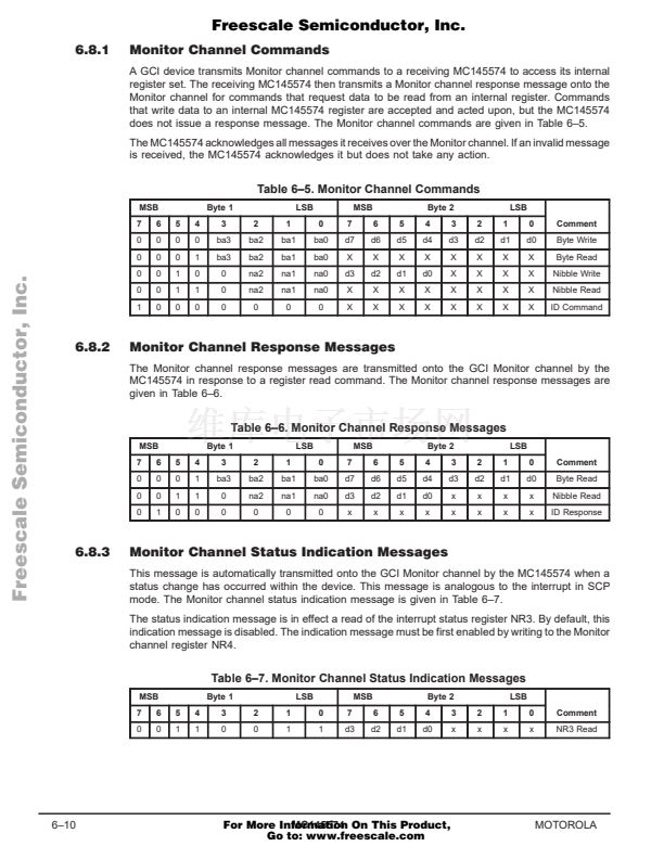
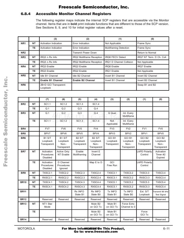
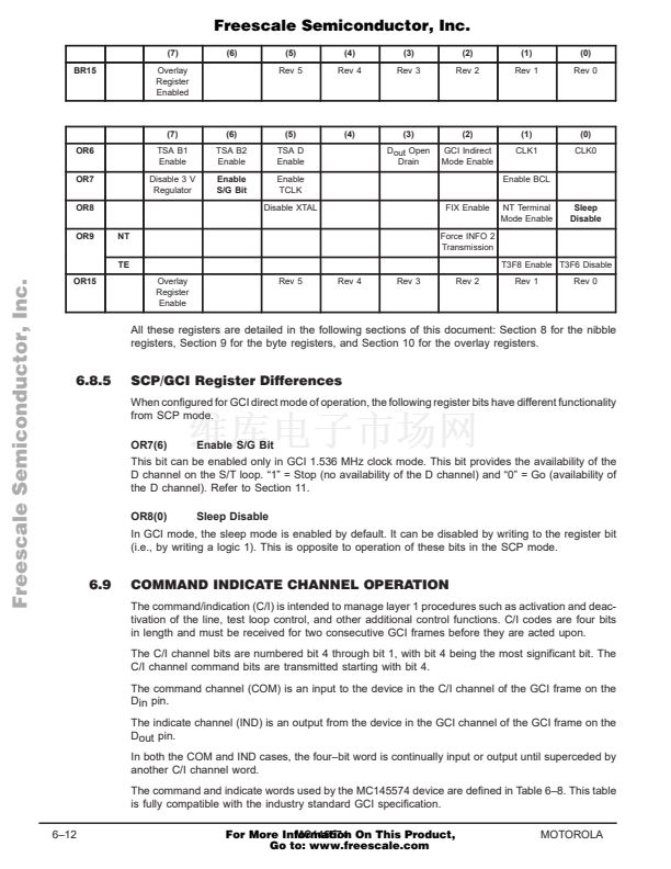
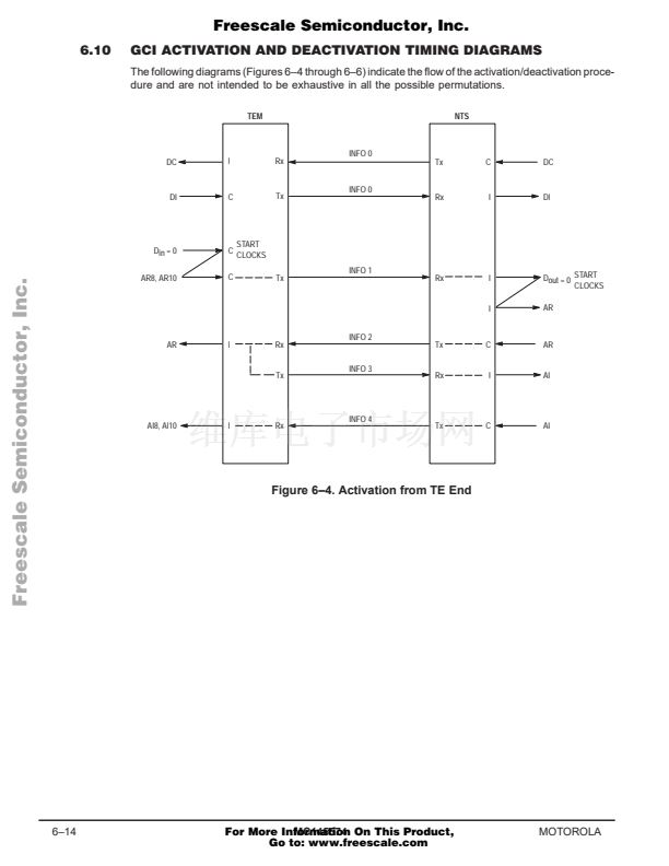
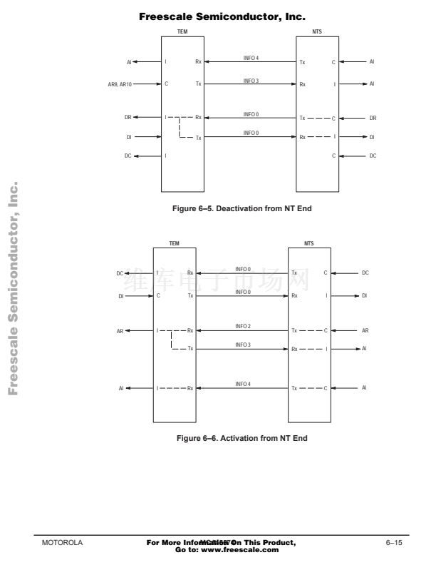
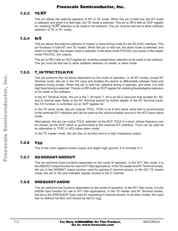
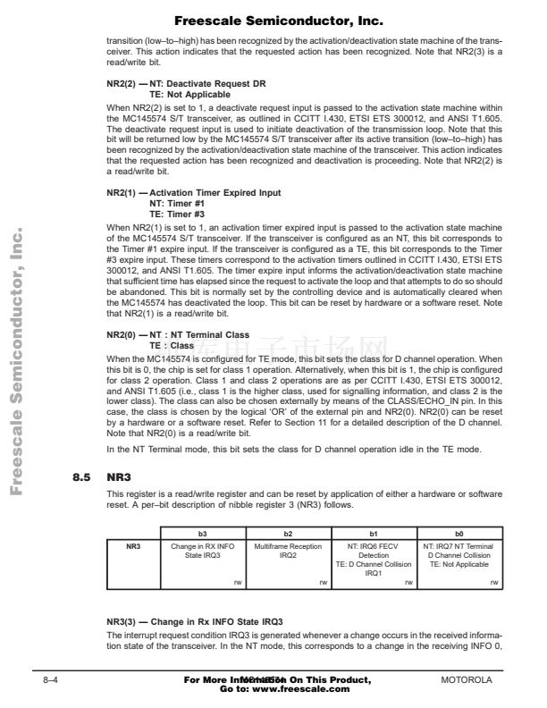
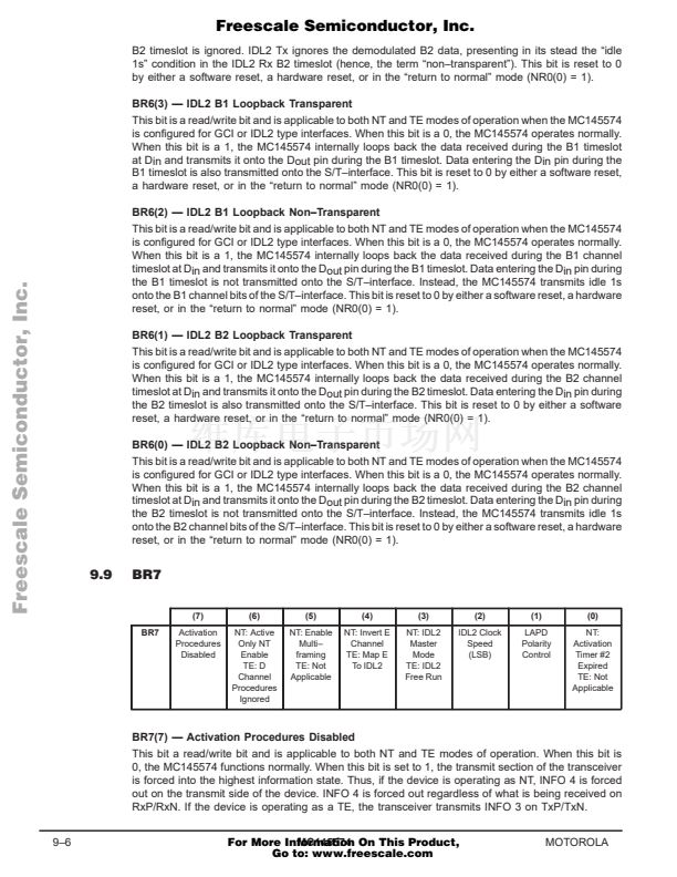
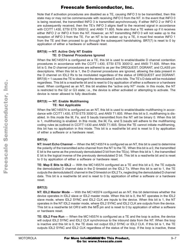
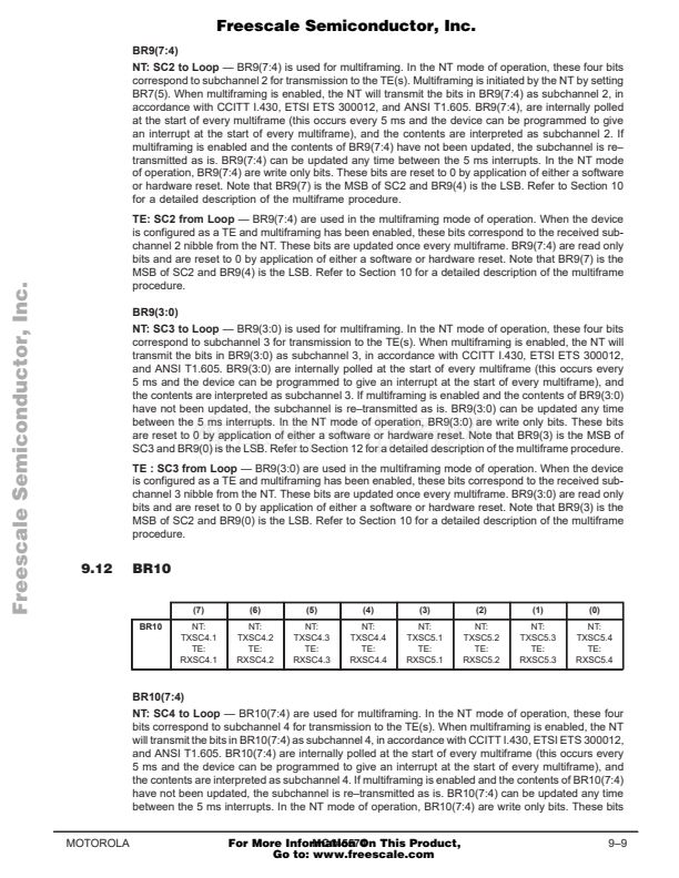
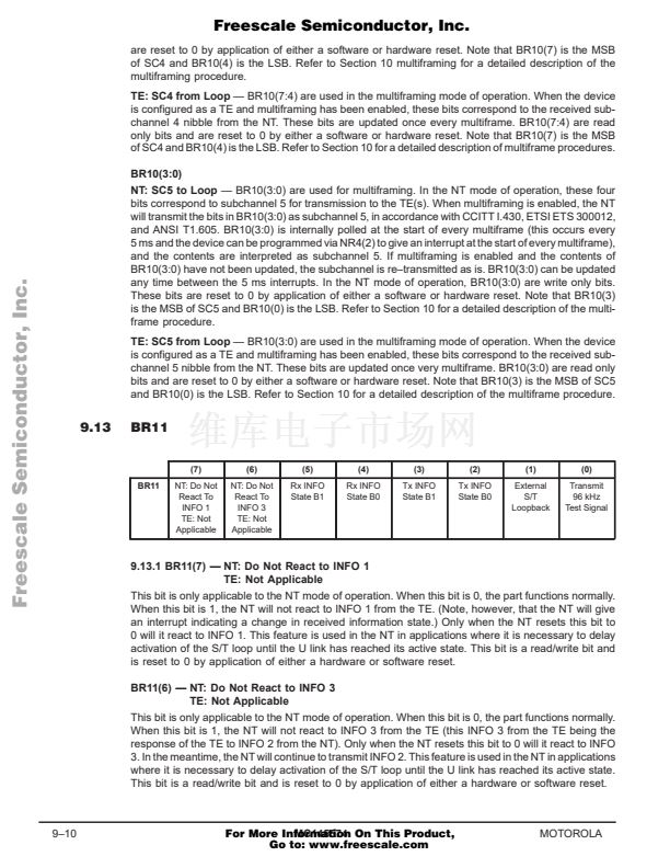
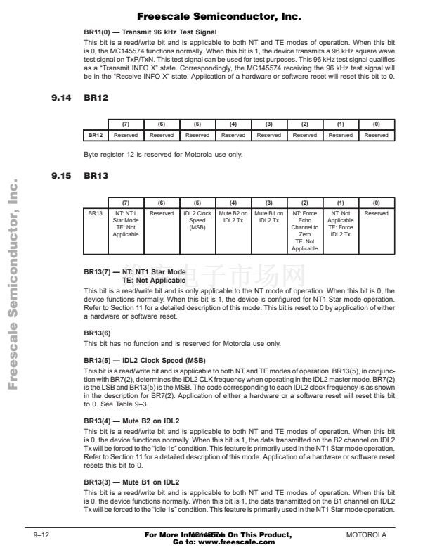
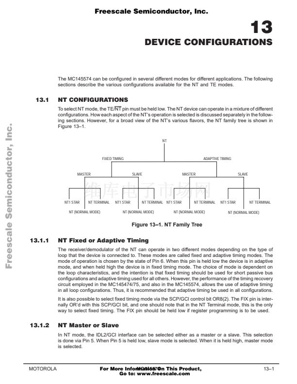
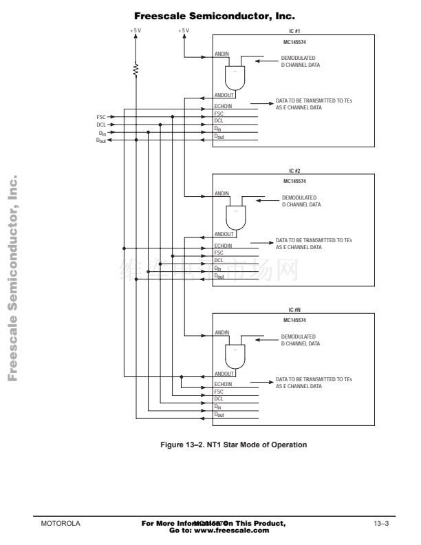
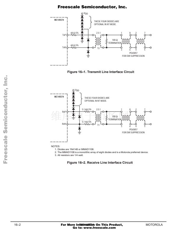
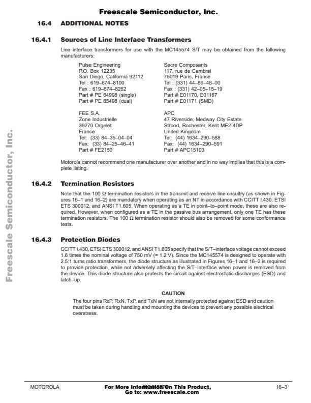
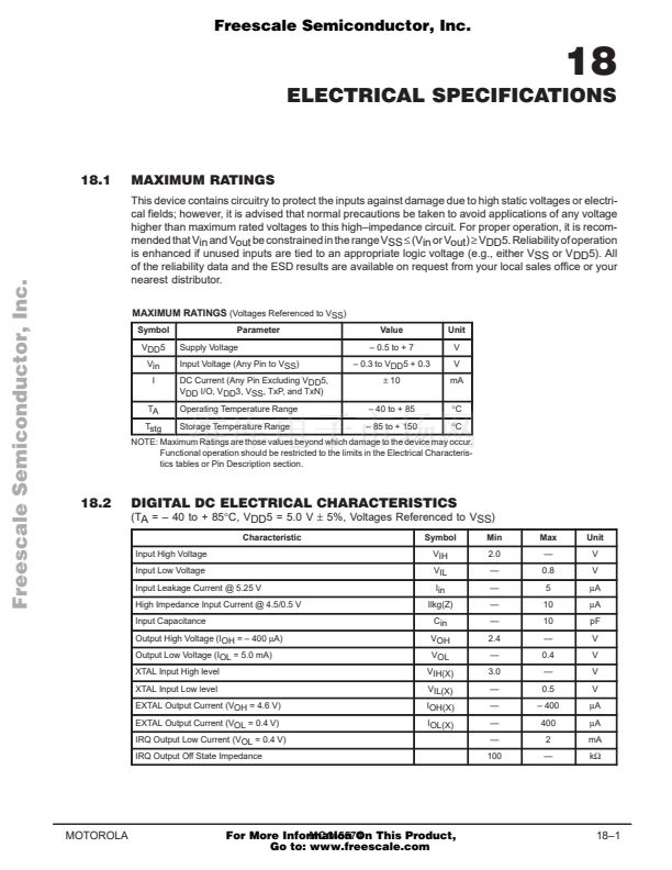
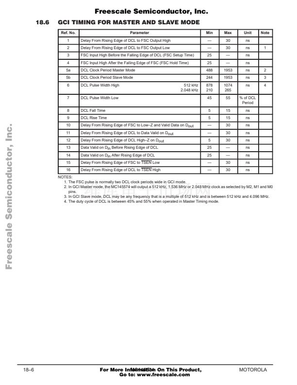
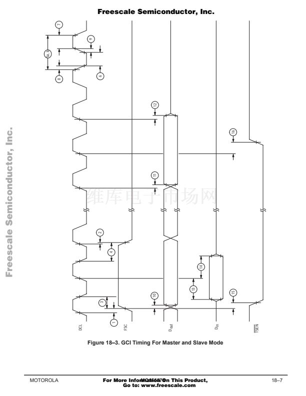
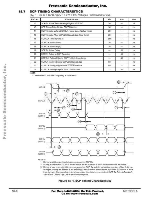
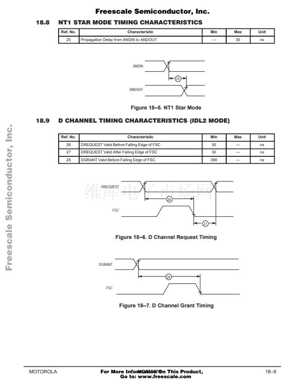
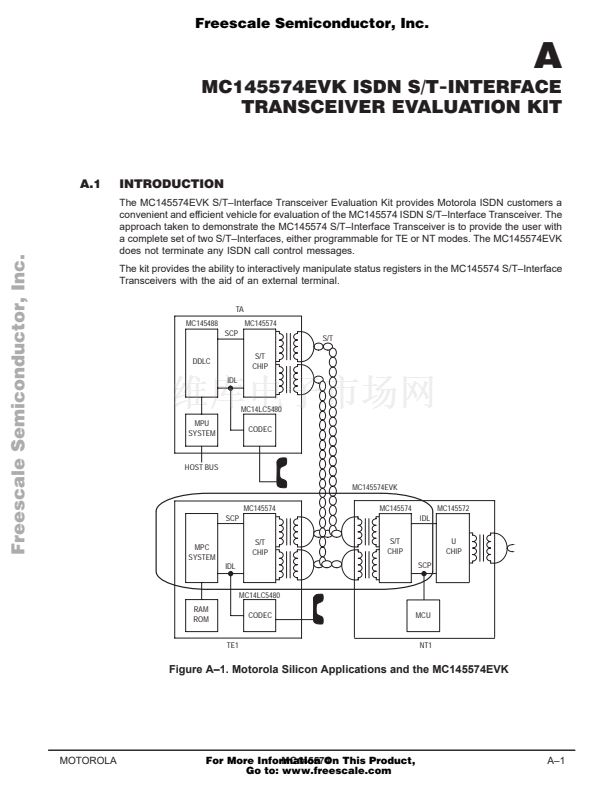
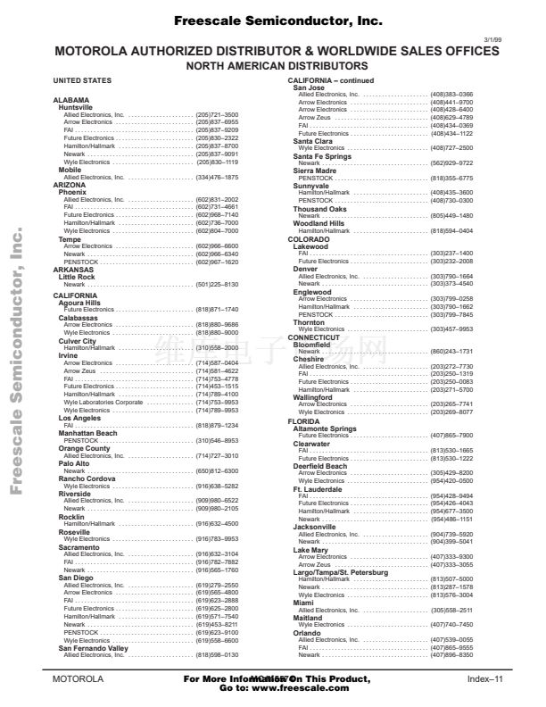
Freescale Semiconductor, Inc.
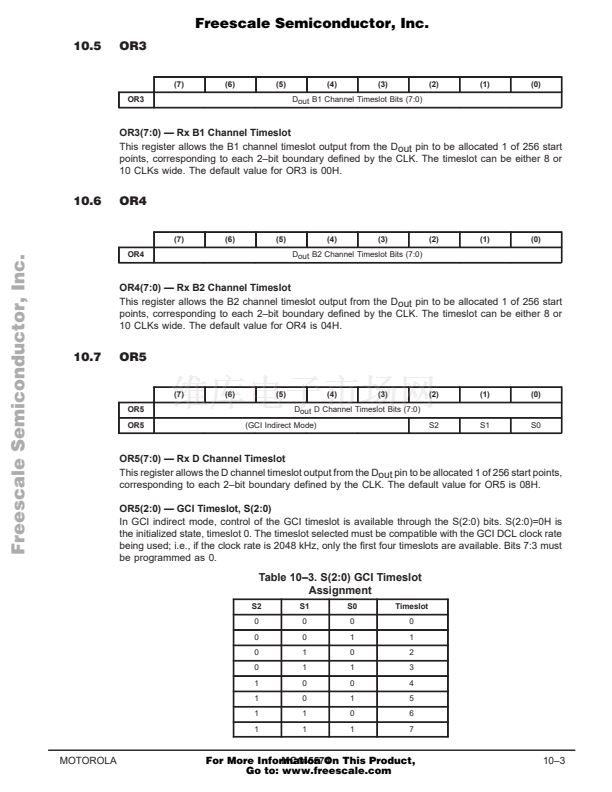
10.5
OR3
(7)
OR3
(6)
(5)
(4)
(3)
(2)
(1)
(0)
Dout B1 Channel Timeslot Bits (7:0)
OR3(7:0) 鈥?Rx B1 Channel Timeslot
This register allows the B1 channel timeslot output from the Dout pin to be allocated 1 of 256 start
points, corresponding to each 2鈥揵it boundary defined by the CLK. The timeslot can be either 8 or
10 CLKs wide. The default value for OR3 is 00H.
10.6
OR4
(7)
OR4
(6)
(5)
(4)
(3)
(2)
(1)
(0)
Freescale Semiconductor, Inc...
Dout B2 Channel Timeslot Bits (7:0)
OR4(7:0) 鈥?Rx B2 Channel Timeslot
This register allows the B2 channel timeslot output from the Dout pin to be allocated 1 of 256 start
points, corresponding to each 2鈥揵it boundary defined by the CLK. The timeslot can be either 8 or
10 CLKs wide. The default value for OR4 is 04H.
10.7
OR5
(7)
OR5
OR5
(6)
(5)
(4)
(3)
(2)
(1)
(0)
Dout D Channel Timeslot Bits (7:0)
(GCI Indirect Mode)
S2
S1
S0
OR5(7:0) 鈥?Rx D Channel Timeslot
This register allows the D channel timeslot output from the Dout pin to be allocated 1 of 256 start points,
corresponding to each 2鈥揵it boundary defined by the CLK. The default value for OR5 is 08H.
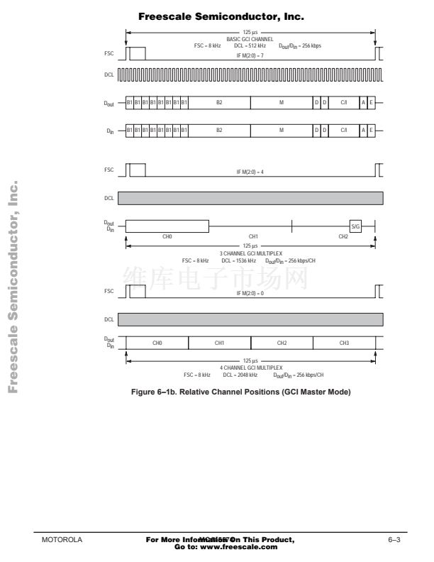
OR5(2:0) 鈥?GCI Timeslot, S(2:0)
In GCI indirect mode, control of the GCI timeslot is available through the S(2:0) bits. S(2:0)=0H is
the initialized state, timeslot 0. The timeslot selected must be compatible with the GCI DCL clock rate
being used; i.e., if the clock rate is 2048 kHz, only the first four timeslots are available. Bits 7:3 must
be programmed as 0.
Table 10鈥?. S(2:0) GCI Timeslot
Assignment
S2
0
0
0
0
1
1
1
1
S1
0
0
1
1
0
0
1
1
S0
0
1
0
1
0
1
0
1
Timeslot
0
1
2
3
4
5
6
7
MOTOROLA
MC145574
For More Information On This Product,
Go to: www.freescale.com
10鈥?


 1
1
 2
2
 3
3
 4
4
 5
5
 6
6
 7
7
 8
8
 9
9
 10
10
 11
11
 12
12
 13
13
 14
14
 15
15
 16
16
 17
17
 18
18
 19
19
 20
20
 21
21
 22
22
 23
23
 24
24
 25
25
 26
26
 27
27
 28
28
 29
29
 30
30
 31
31
 32
32
 33
33
 34
34
 35
35
 36
36
 37
37
 38
38
 39
39
 40
40
 41
41
 42
42
 43
43
 44
44
 45
45
 46
46
 47
47
 48
48
 49
49
 50
50
 51
51
 52
52
 53
53
 54
54
 55
55
 56
56
 57
57
 58
58
 59
59
 60
60
 61
61
 62
62
 63
63
 64
64
 65
65
 66
66
 67
67
 68
68
 69
69
 70
70
 71
71
 72
72
 73
73
 74
74
 75
75
 76
76
 77
77
 78
78
 79
79
 80
80
 81
81
 82
82
 83
83
 84
84
 85
85
 86
86
 87
87
 88
88
 89
89
 90
90
 91
91
 92
92
 93
93
 94
94
 95
95
 96
96
 97
97
 98
98
 99
99
 100
100
 101
101
 102
102
 103
103
 104
104
 105
105
 106
106
 107
107
 108
108
 109
109
 110
110
 111
111
 112
112
 113
113
 114
114
 115
115
 116
116
 117
117
 118
118
 119
119
 120
120
 121
121
 122
122
 123
123
 124
124
 125
125
 126
126
 127
127
 128
128
 129
129
 130
130
 131
131
 132
132
 133
133
 134
134
 135
135
 136
136
 137
137
 138
138
 139
139
 140
140
 141
141
 142
142
 143
143
 144
144
 145
145
 146
146
 147
147
 148
148
 149
149
 150
150
 151
151
 152
152
 153
153
 154
154
 155
155
 156
156
 157
157
 158
158
 159
159
 160
160
 161
161
 162
162
 163
163
 164
164
