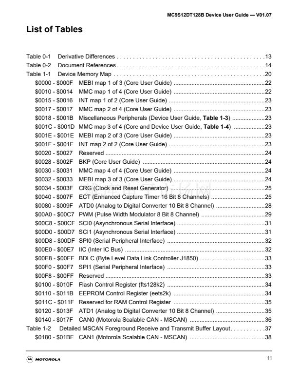
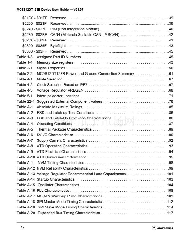
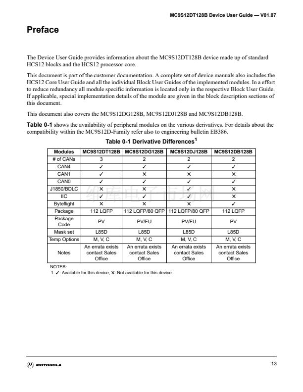
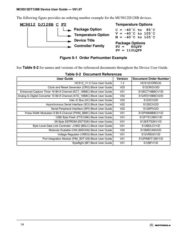
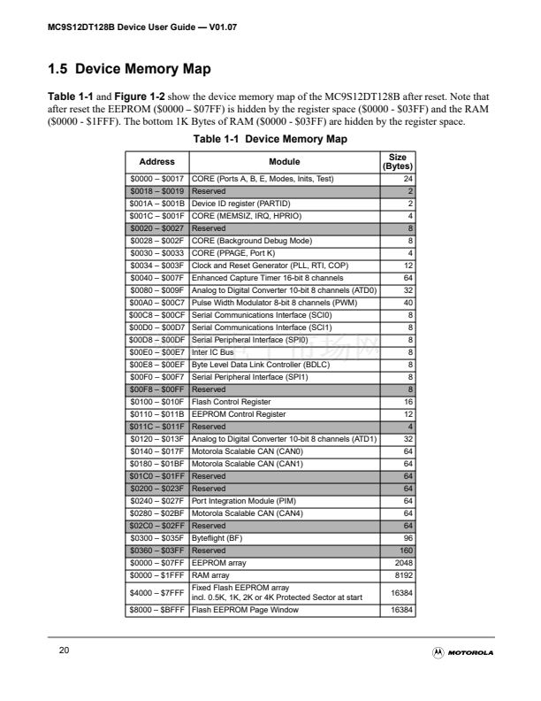
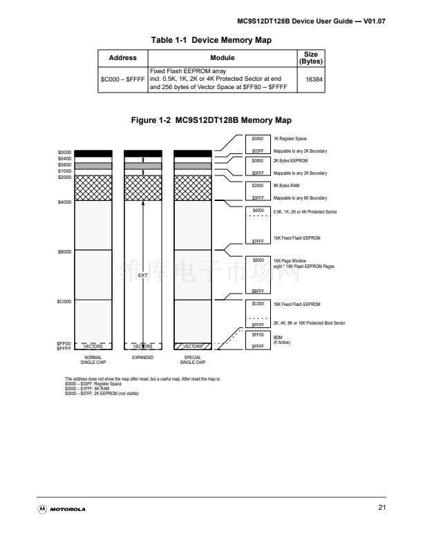
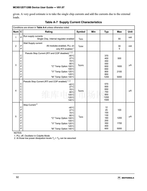
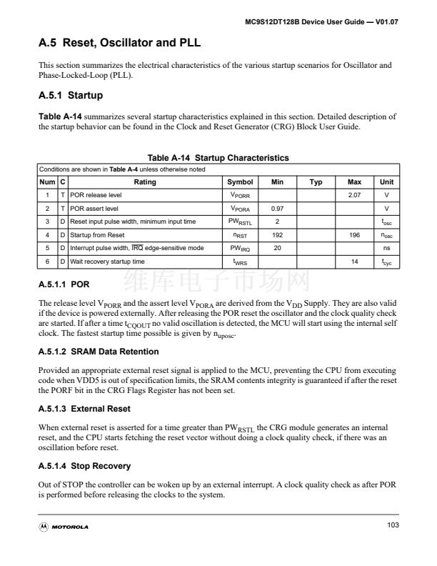
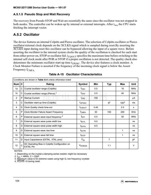
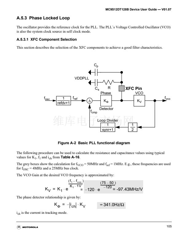
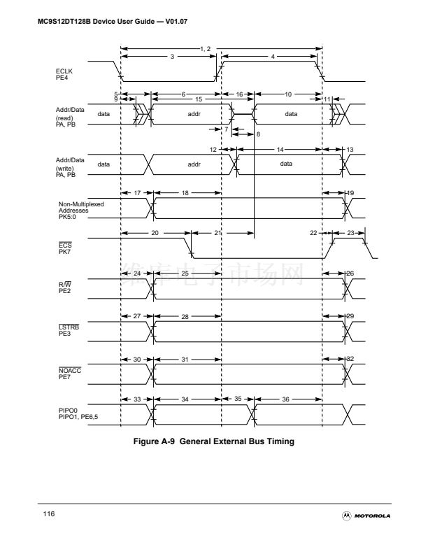
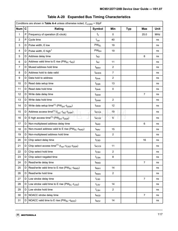
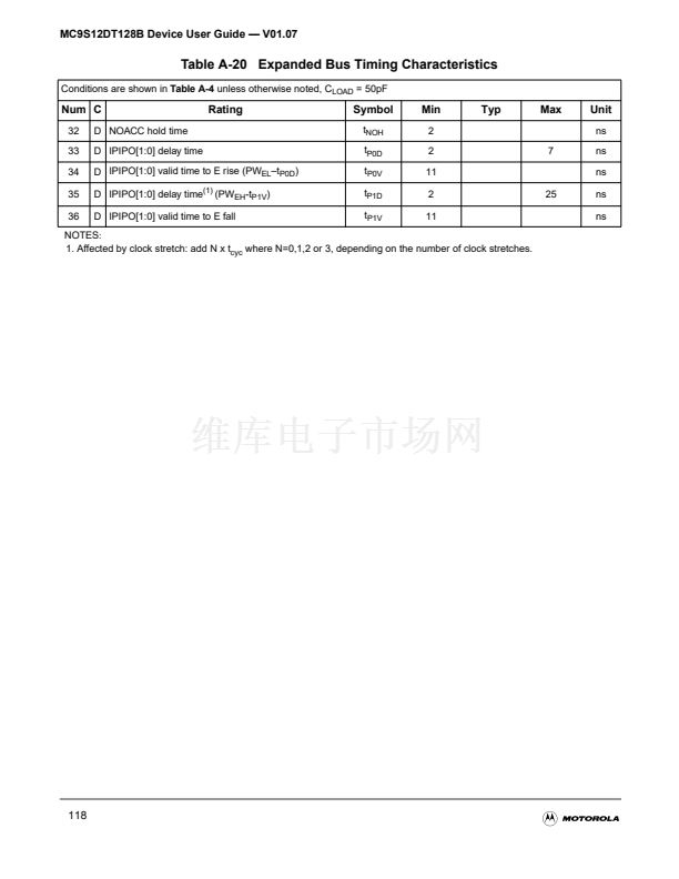
show the device memory map of the MC9S12DT128B after reset. Note that
鈥?/div>
$07FF) is hidden by the register space ($0000 - $03FF) and the RAM
($0000 - $1FFF). The bottom 1K Bytes of RAM ($0000 - $03FF) are hidden by the register space.
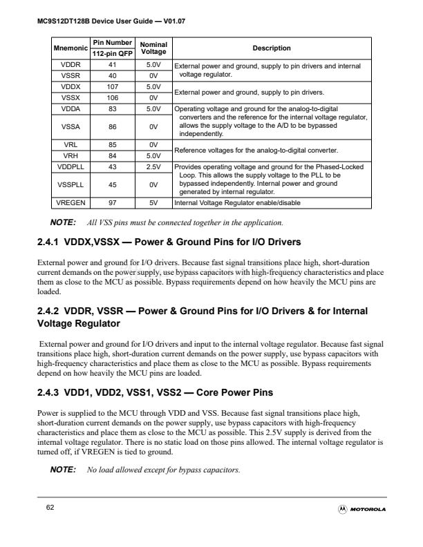
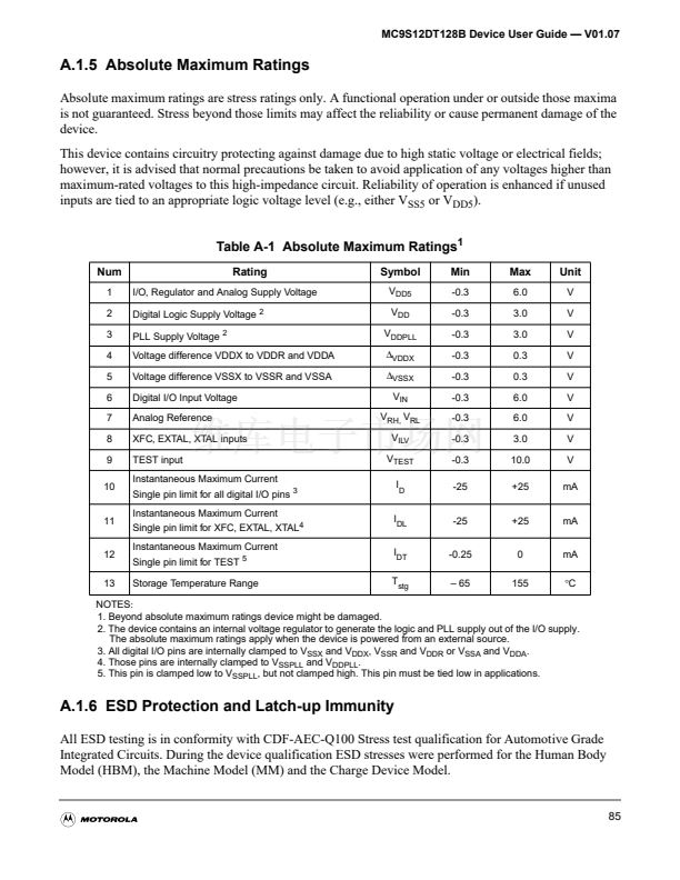
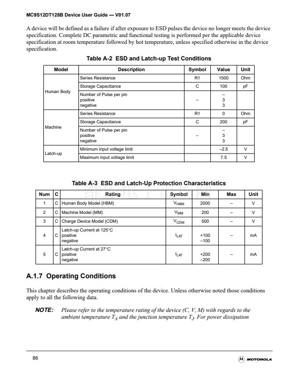
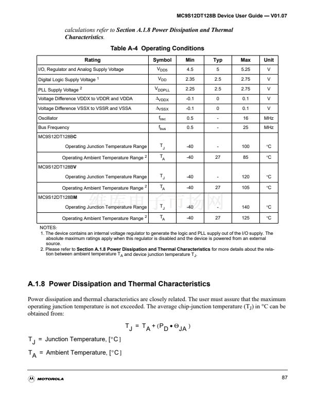
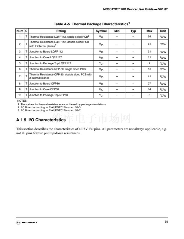
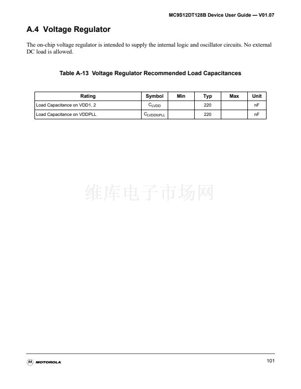
Table 1-1 Device Memory Map
Address
$0000 鈥?$0017
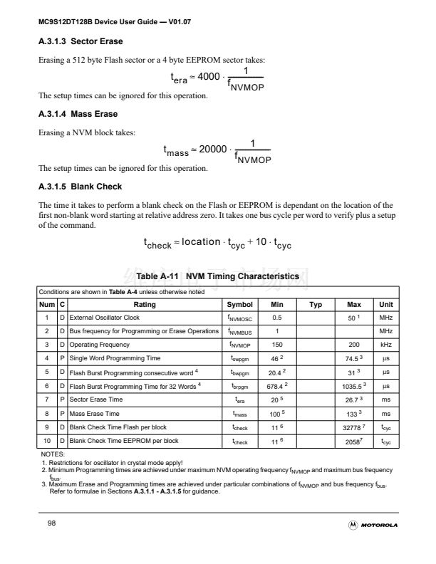
$0018 鈥?$0019
Reserved
Module
CORE (Ports A, B, E, Modes, Inits, Test)
Size
(Bytes)
24
2
2
4
8
8
4
12
64
32
40
8
8
8
8
8
8
8
16
12
4
32
64
64
64
64
64
64
64
96
160
2048
8192
16384
16384
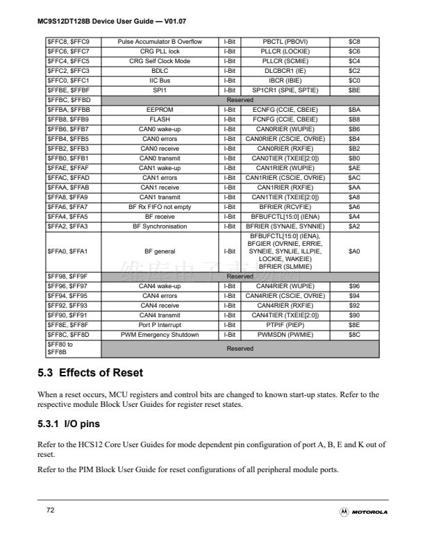
$001A 鈥?$001B Device ID register (PARTID)
$001C 鈥?$001F CORE (MEMSIZ, IRQ, HPRIO)
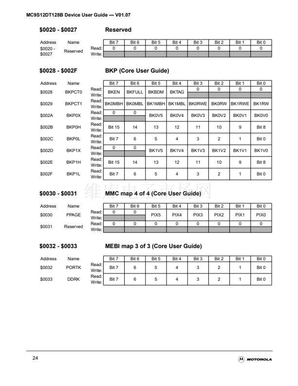
$0020 鈥?$0027
$0030 鈥?$0033
Reserved
CORE (PPAGE, Port K)
$0028 鈥?$002F CORE (Background Debug Mode)
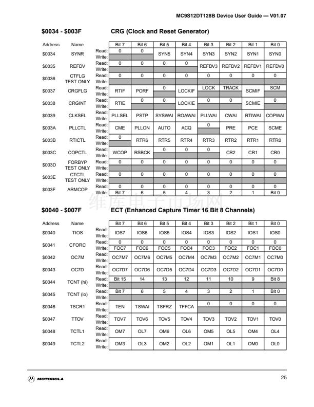
$0034 鈥?$003F Clock and Reset Generator (PLL, RTI, COP)
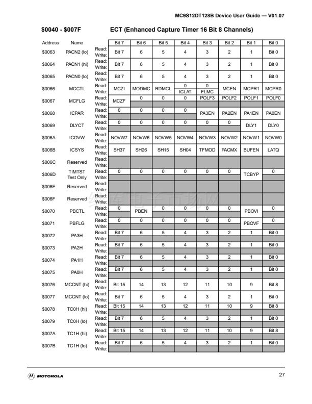
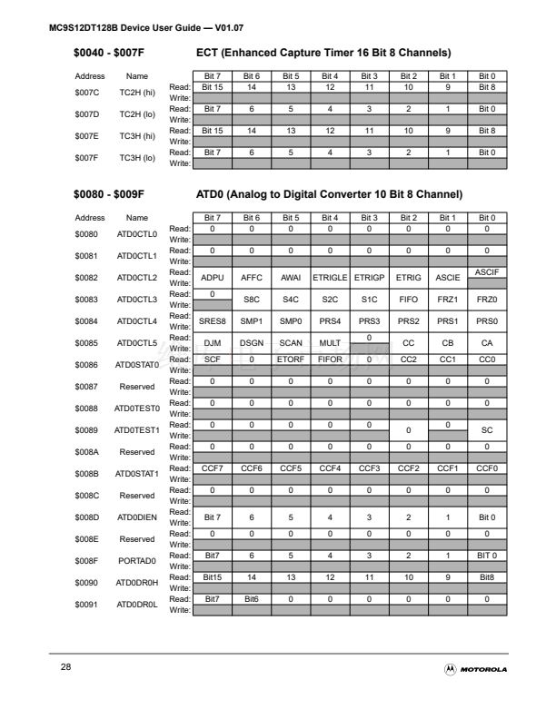
$0040 鈥?$007F Enhanced Capture Timer 16-bit 8 channels
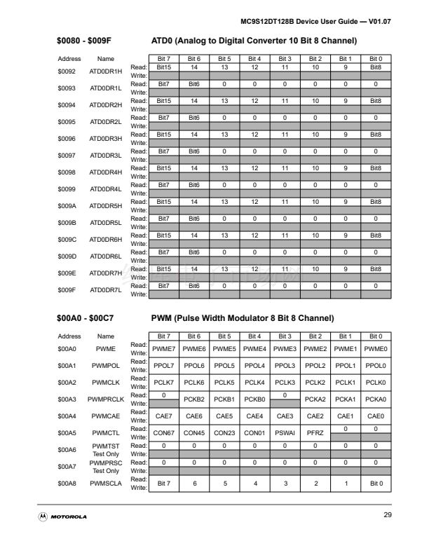
$0080 鈥?$009F Analog to Digital Converter 10-bit 8 channels (ATD0)
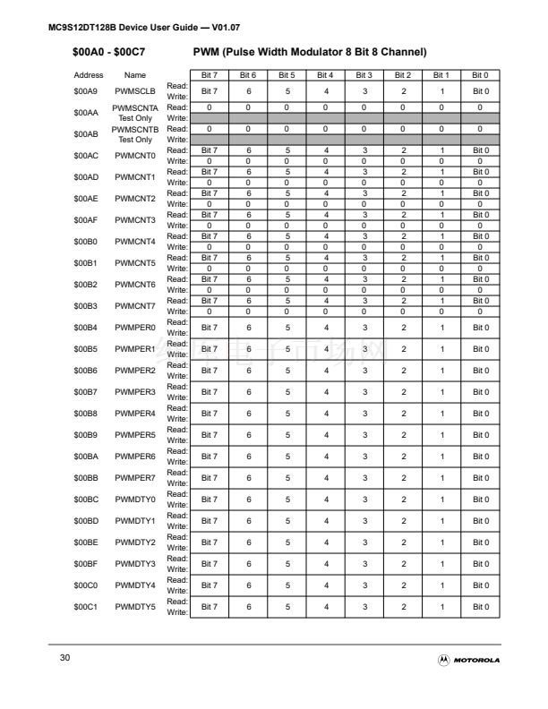
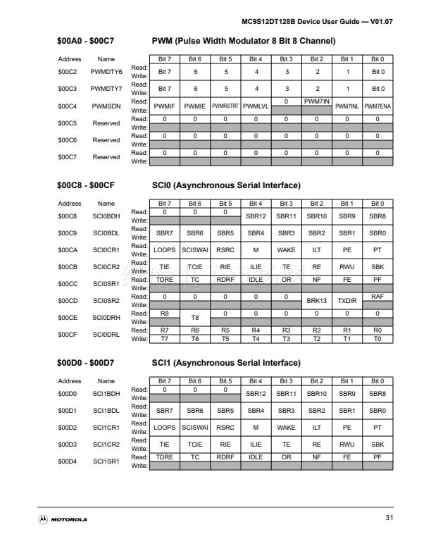
$00A0 鈥?$00C7 Pulse Width Modulator 8-bit 8 channels (PWM)
$00C8 鈥?$00CF Serial Communications Interface (SCI0)
$00D0 鈥?$00D7 Serial Communications Interface (SCI1)
$00D8 鈥?$00DF Serial Peripheral Interface (SPI0)
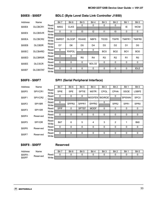
$00E0 鈥?$00E7 Inter IC Bus
$00E8 鈥?$00EF Byte Level Data Link Controller (BDLC)
$00F0 鈥?$00F7 Serial Peripheral Interface (SPI1)
$00F8 鈥?$00FF Reserved
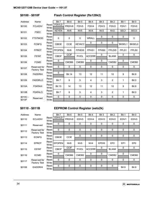
$0100 鈥?$010F Flash Control Register
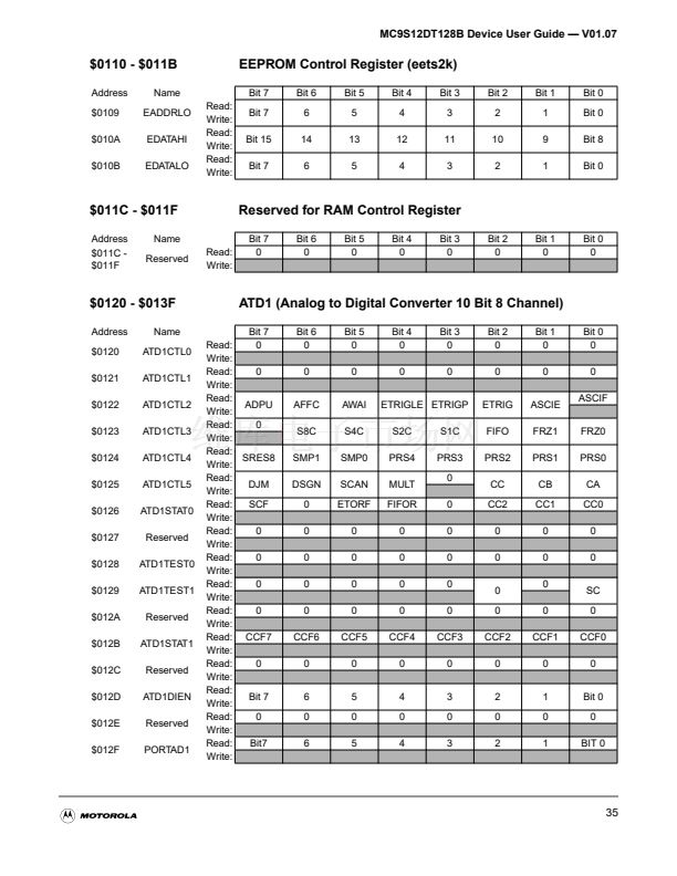
$0110 鈥?$011B EEPROM Control Register
$011C 鈥?$011F Reserved
$0120 鈥?$013F Analog to Digital Converter 10-bit 8 channels (ATD1)
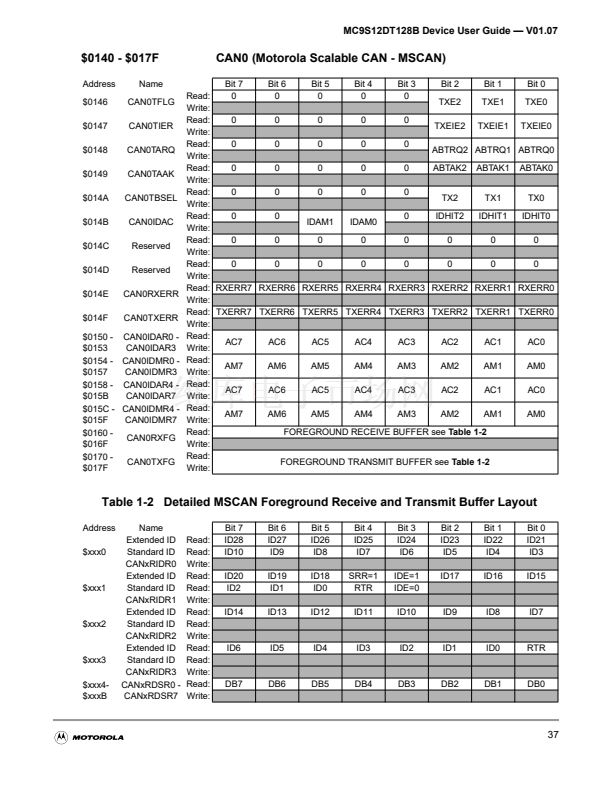
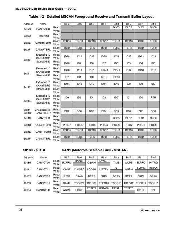
$0140 鈥?$017F Motorola Scalable CAN (CAN0)
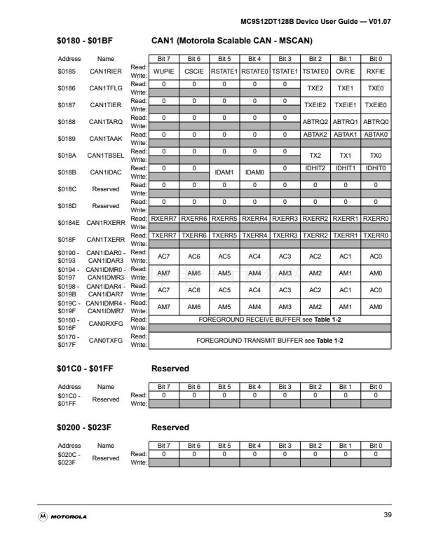
$0180 鈥?$01BF Motorola Scalable CAN (CAN1)
$01C0 鈥?$01FF Reserved
$0200 鈥?$023F Reserved
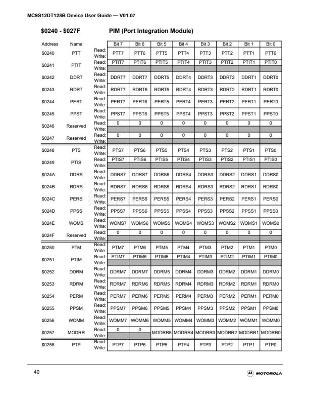
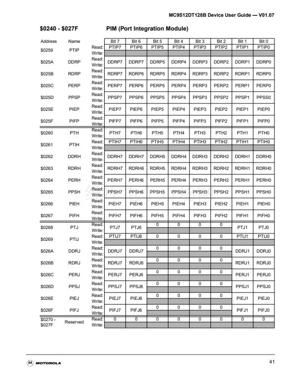
$0240 鈥?$027F Port Integration Module (PIM)
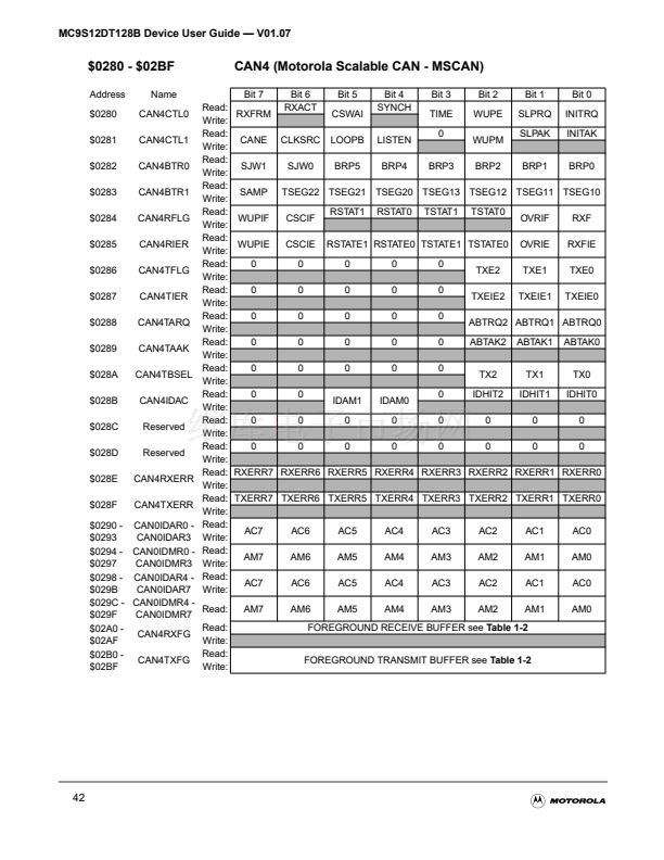
$0280 鈥?$02BF Motorola Scalable CAN (CAN4)
$02C0 鈥?$02FF Reserved
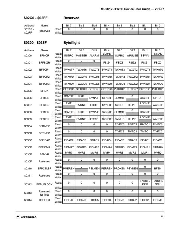
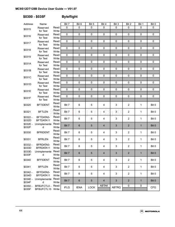
$0300 鈥?$035F Byte铿俰ght (BF)
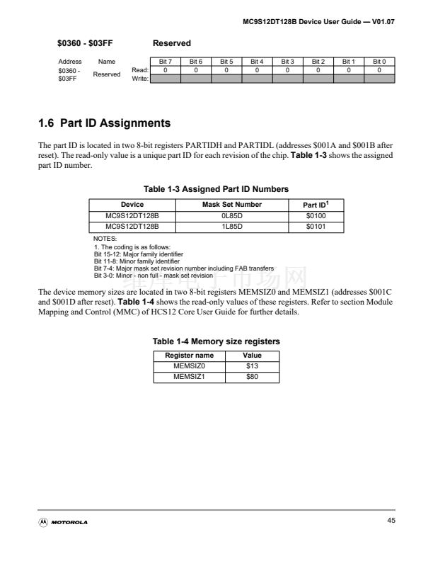
$0360 鈥?$03FF Reserved
$0000 鈥?$07FF EEPROM array
$0000 鈥?$1FFF RAM array
$4000 鈥?$7FFF
Fixed Flash EEPROM array
incl. 0.5K, 1K, 2K or 4K Protected Sector at start
$8000 鈥?$BFFF Flash EEPROM Page Window
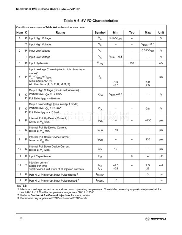
20


 1
1
 2
2
 3
3
 4
4
 5
5
 6
6
 7
7
 8
8
 9
9
 10
10
 11
11
 12
12
 13
13
 14
14
 15
15
 16
16
 17
17
 18
18
 19
19
 20
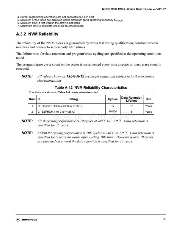
20
 21
21
 22
22
 23
23
 24
24
 25
25
 26
26
 27
27
 28
28
 29
29
 30
30
 31
31
 32
32
 33
33
 34
34
 35
35
 36
36
 37
37
 38
38
 39
39
 40
40
 41
41
 42
42
 43
43
 44
44
 45
45
 46
46
 47
47
 48
48
 49
49
 50
50
 51
51
 52
52
 53
53
 54
54
 55
55
 56
56
 57
57
 58
58
 59
59
 60
60
 61
61
 62
62
 63
63
 64
64
 65
65
 66
66
 67
67
 68
68
 69
69
 70
70
 71
71
 72
72
 73
73
 74
74
 75
75
 76
76
 77
77
 78
78
 79
79
 80
80
 81
81
 82
82
 83
83
 84
84
 85
85
 86
86
 87
87
 88
88
 89
89
 90
90
 91
91
 92
92
 93
93
 94
94
 95
95
 96
96
 97
97
 98
98
 99
99
 100
100
 101
101
 102
102
 103
103
 104
104
 105
105
 106
106
 107
107
 108
108
 109
109
 110
110
 111
111
 112
112
 113
113
 114
114
 115
115
 116
116
 117
117
 118
118
 119
119
 120
120
 121
121
 122
122
 123
123
 124
124
