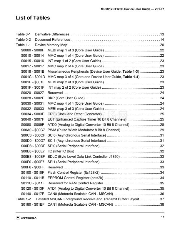
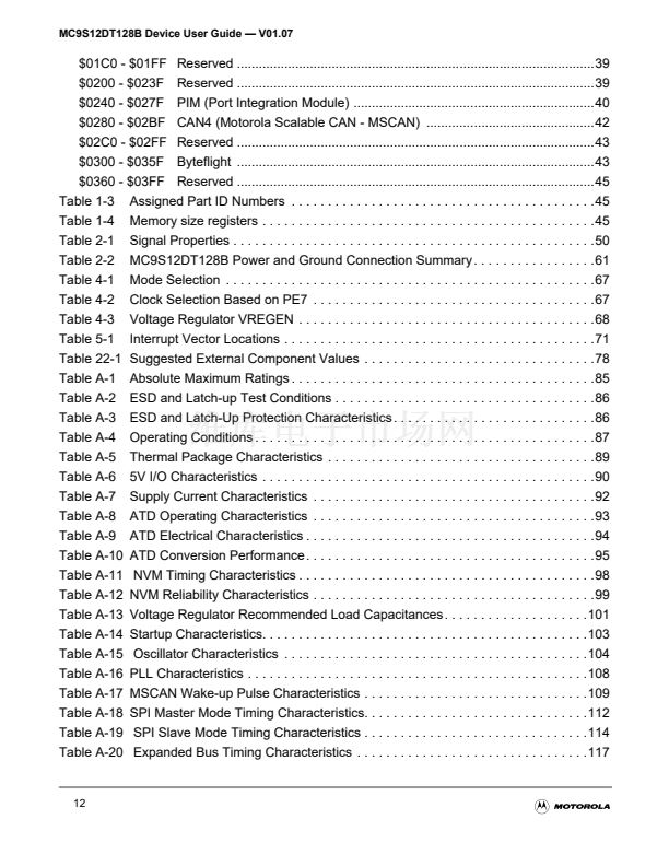
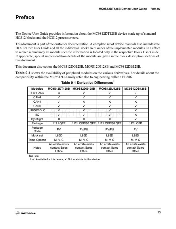
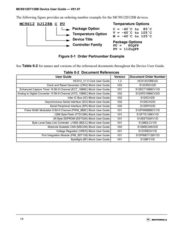
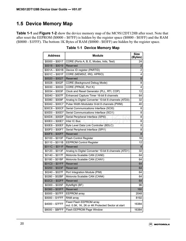
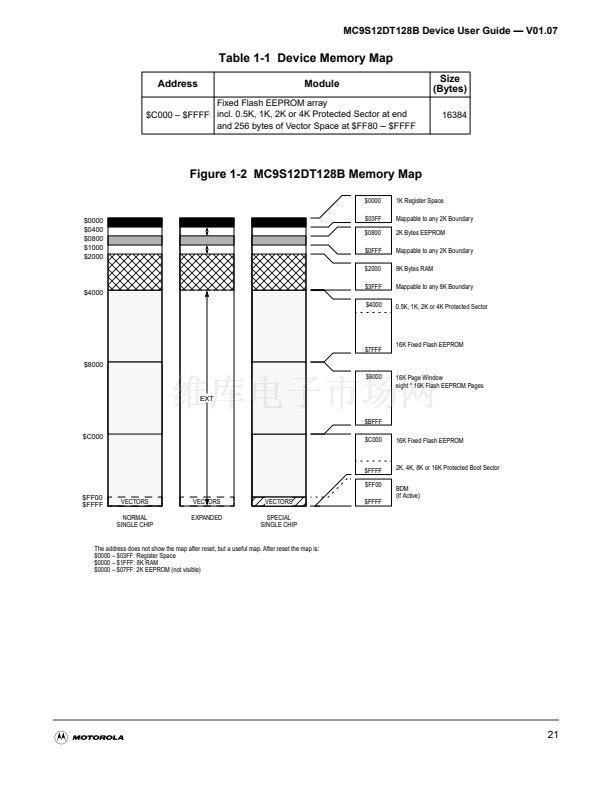
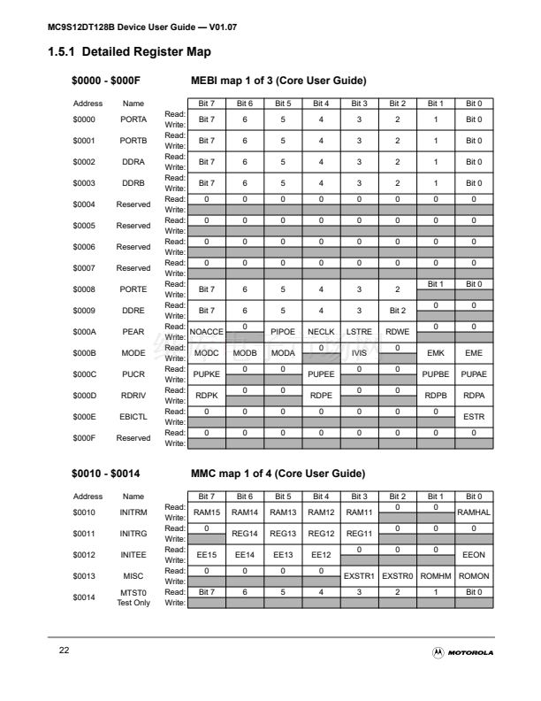
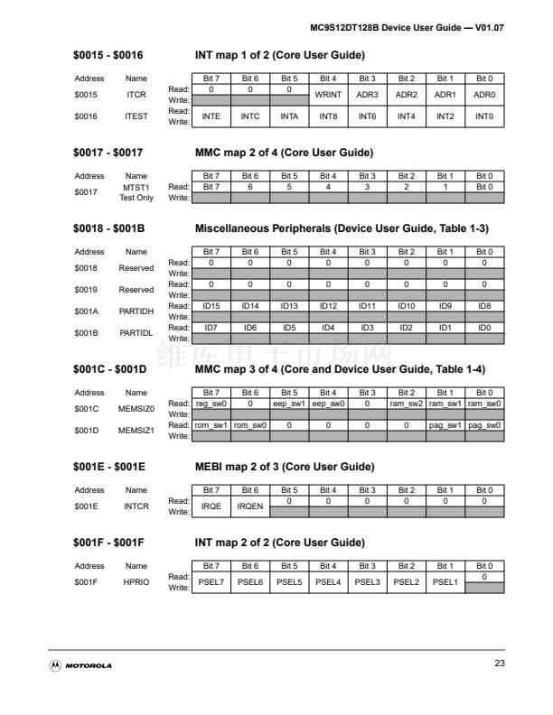
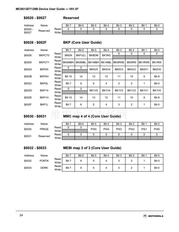
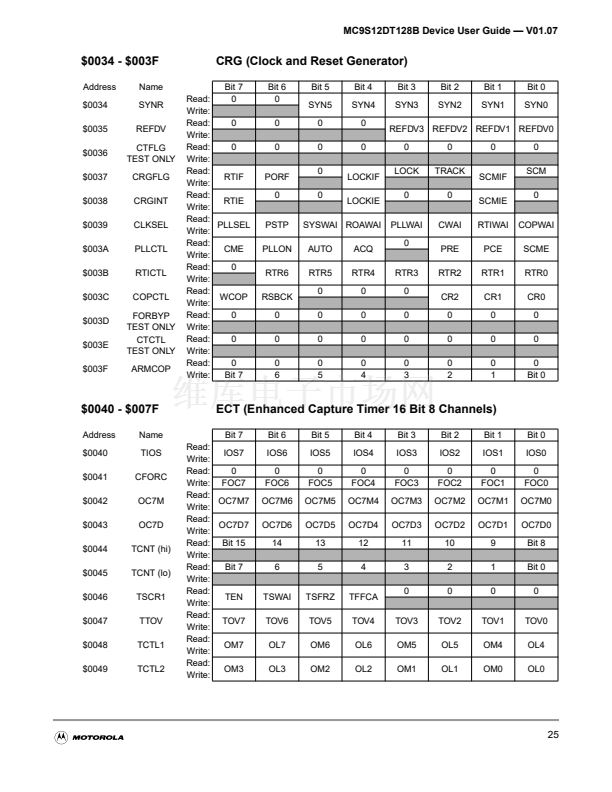
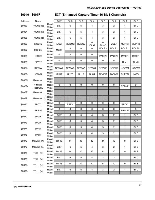
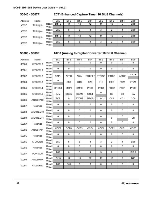
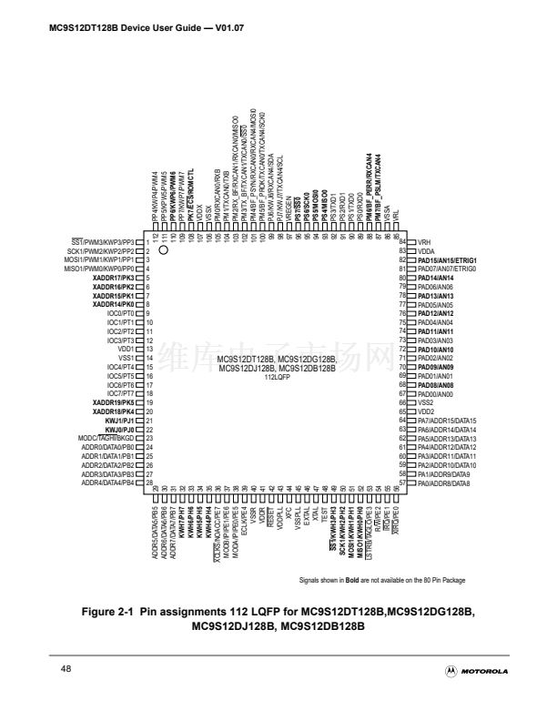
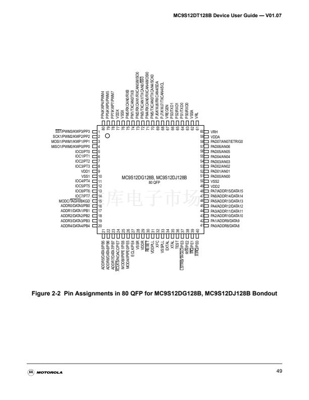
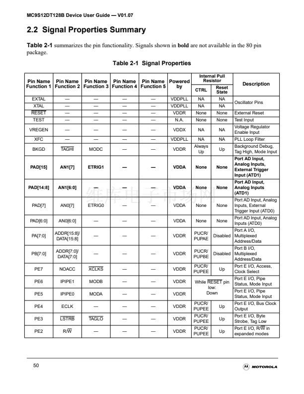
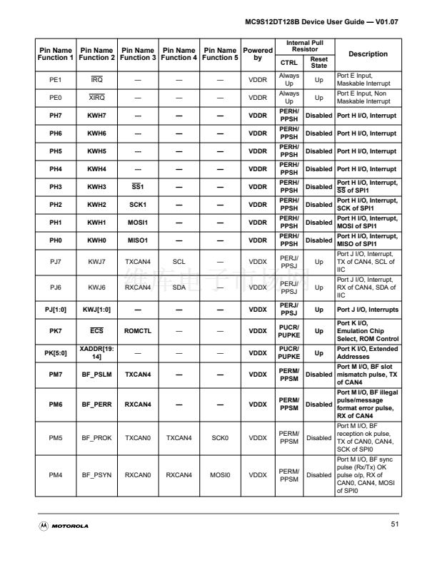
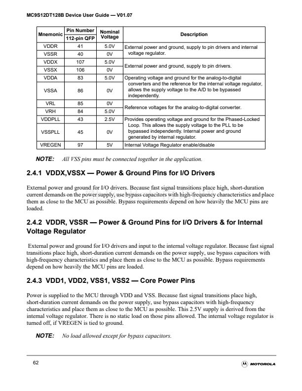
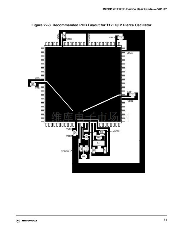
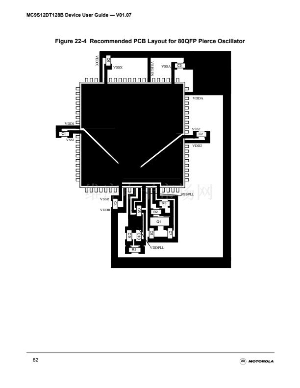
MC9S12DT128B Device User Guide 鈥?V01.07
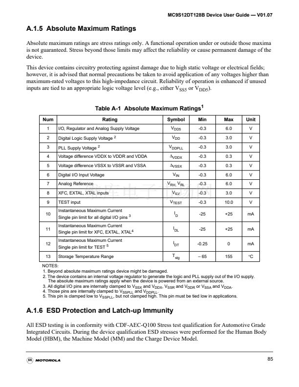
A.1.5 Absolute Maximum Ratings
Absolute maximum ratings are stress ratings only. A functional operation under or outside those maxima
is not guaranteed. Stress beyond those limits may affect the reliability or cause permanent damage of the
device.
This device contains circuitry protecting against damage due to high static voltage or electrical fields;
however, it is advised that normal precautions be taken to avoid application of any voltages higher than
maximum-rated voltages to this high-impedance circuit. Reliability of operation is enhanced if unused
inputs are tied to an appropriate logic voltage level (e.g., either V
SS5
or V
DD5
).
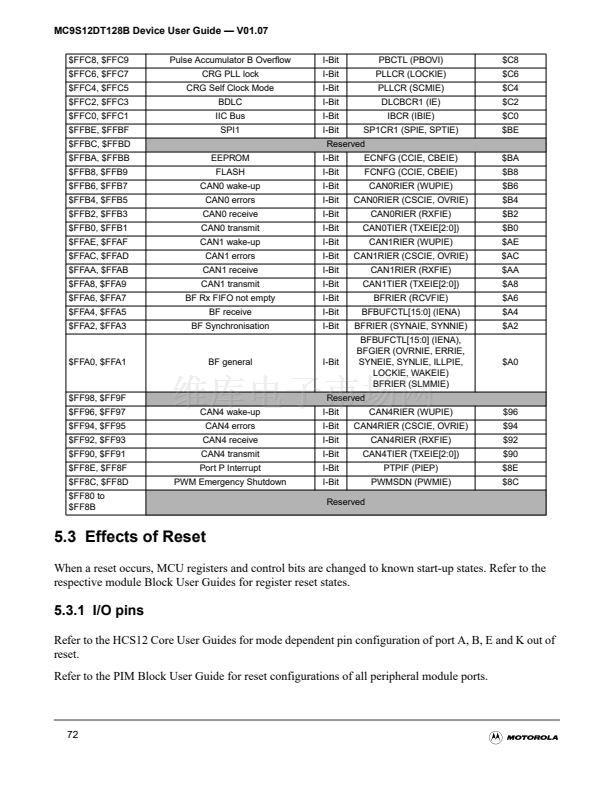
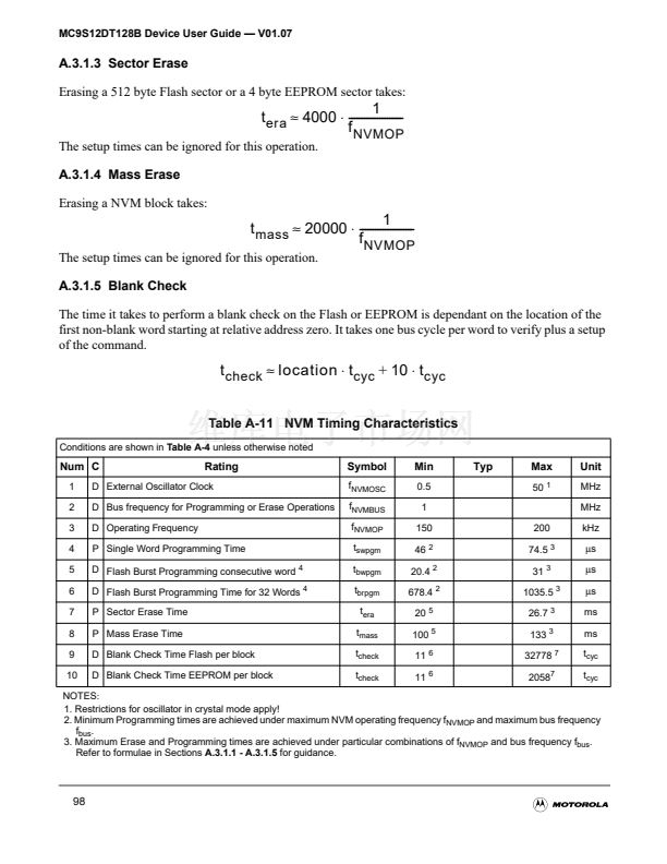
Table A-1 Absolute Maximum Ratings
1
Num
1
2
3
4
5
6
7
8
9
10
11
12
13
Rating
I/O, Regulator and Analog Supply Voltage
Digital Logic Supply Voltage
2
PLL Supply Voltage
2
Voltage difference VDDX to VDDR and VDDA
Voltage difference VSSX to VSSR and VSSA
Digital I/O Input Voltage
Analog Reference
XFC, EXTAL, XTAL inputs
TEST input
Instantaneous Maximum Current
Single pin limit for all digital I/O pins
3
Instantaneous Maximum Current
Single pin limit for XFC, EXTAL, XTAL
4
Instantaneous Maximum Current
Single pin limit for TEST
5
Storage Temperature Range
Symbol
V
DD5
V
DD
V
DDPLL
鈭?/div>
VDDX
鈭?/div>
VSSX
V
IN
V
RH,
V
RL
V
ILV
V
TEST
I
D
I
Min
-0.3
-0.3
-0.3
-0.3
-0.3
-0.3
-0.3
-0.3
-0.3
-25
-25
-0.25
鈥?65
Max
6.0
3.0
3.0
0.3
0.3
6.0
6.0
3.0
10.0
+25
+25
0
155
Unit
V
V
V
V
V
V
V
V
V
mA
mA
mA
掳C
DL
I
DT
T
stg
NOTES:
1. Beyond absolute maximum ratings device might be damaged.
2. The device contains an internal voltage regulator to generate the logic and PLL supply out of the I/O supply.
The absolute maximum ratings apply when the device is powered from an external source.
3. All digital I/O pins are internally clamped to V
SSX
and V
DDX
, V
SSR
and V
DDR
or V
SSA
and V
DDA
.
4. Those pins are internally clamped to V
SSPLL
and V
DDPLL
.
5. This pin is clamped low to V
SSPLL
, but not clamped high. This pin must be tied low in applications.
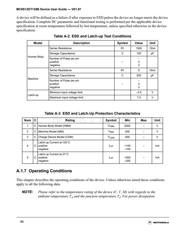
A.1.6 ESD Protection and Latch-up Immunity
All ESD testing is in conformity with CDF-AEC-Q100 Stress test qualification for Automotive Grade
Integrated Circuits. During the device qualification ESD stresses were performed for the Human Body
Model (HBM), the Machine Model (MM) and the Charge Device Model.
85


 1
1
 2
2
 3
3
 4
4
 5
5
 6
6
 7
7
 8
8
 9
9
 10
10
 11
11
 12
12
 13
13
 14
14
 15
15
 16
16
 17
17
 18
18
 19
19
 20
20
 21
21
 22
22
 23
23
 24
24
 25
25
 26
26
 27
27
 28
28
 29
29
 30
30
 31
31
 32
32
 33
33
 34
34
 35
35
 36
36
 37
37
 38
38
 39
39
 40
40
 41
41
 42
42
 43
43
 44
44
 45
45
 46
46
 47
47
 48
48
 49
49
 50
50
 51
51
 52
52
 53
53
 54
54
 55
55
 56
56
 57
57
 58
58
 59
59
 60
60
 61
61
 62
62
 63
63
 64
64
 65
65
 66
66
 67
67
 68
68
 69
69
 70
70
 71
71
 72
72
 73
73
 74
74
 75
75
 76
76
 77
77
 78
78
 79
79
 80
80
 81
81
 82
82
 83
83
 84
84
 85
85
 86
86
 87
87
 88
88
 89
89
 90
90
 91
91
 92
92
 93
93
 94
94
 95
95
 96
96
 97
97
 98
98
 99
99
 100
100
 101
101
 102
102
 103
103
 104
104
 105
105
 106
106
 107
107
 108
108
 109
109
 110
110
 111
111
 112
112
 113
113
 114
114
 115
115
 116
116
 117
117
 118
118
 119
119
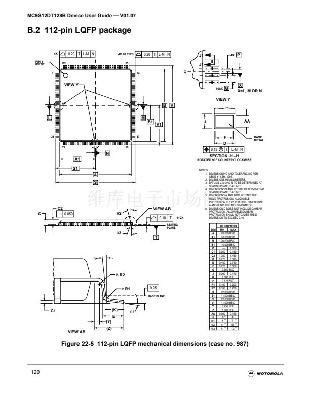 120
120
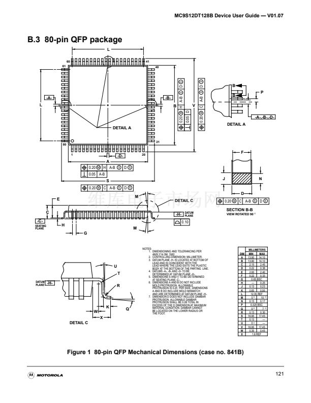 121
121
 122
122
 123
123
 124
124
