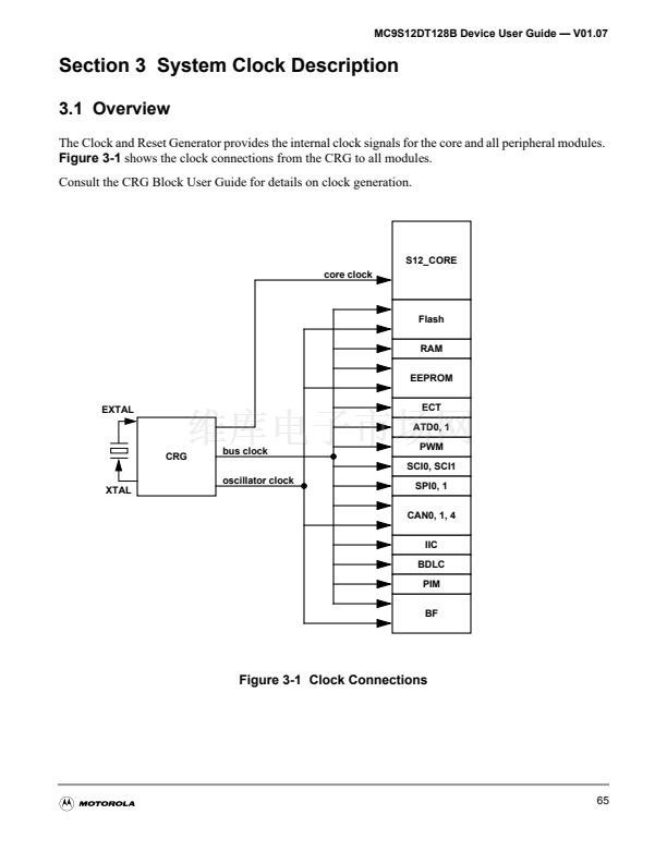
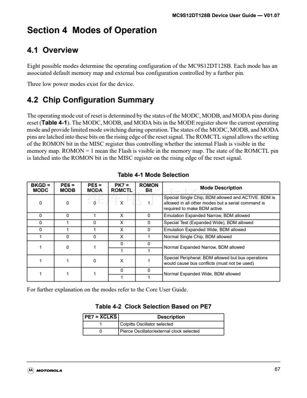
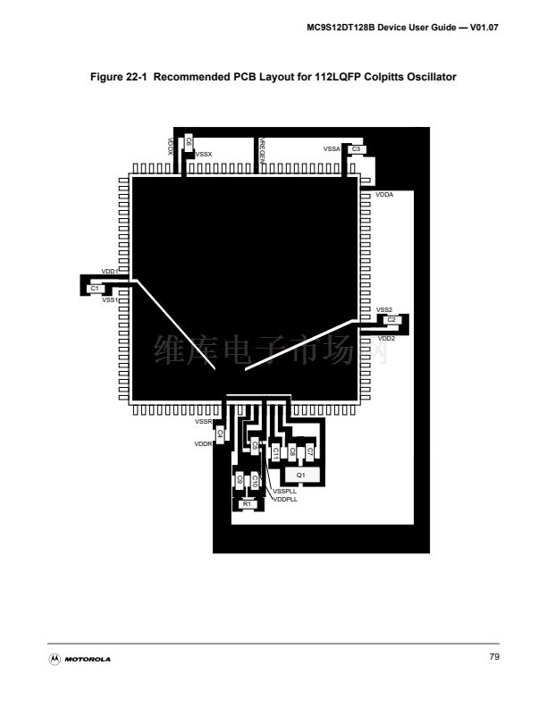
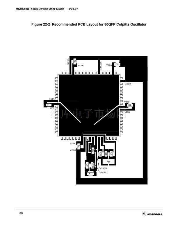
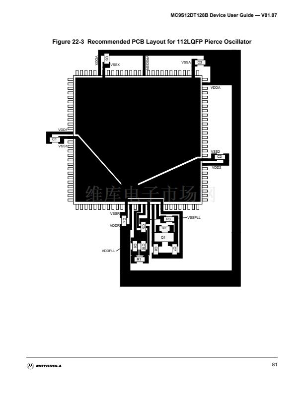
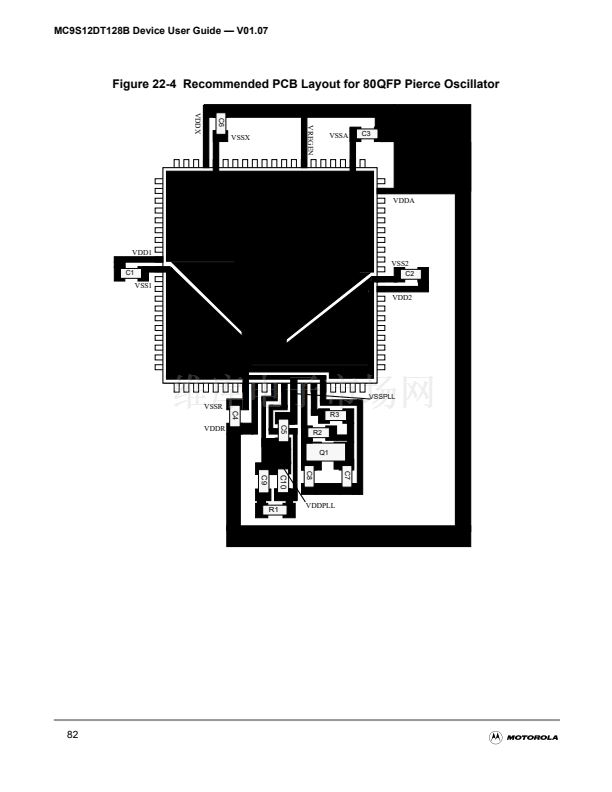
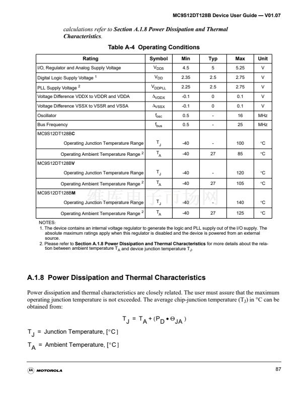
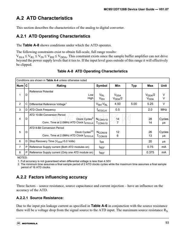
鈮?/div>
V
DDA
.
This constraint exists since the sample buffer amplifier can not drive
beyond the power supply levels that it ties to. If the input level goes outside of this range it will effectively
be clipped.
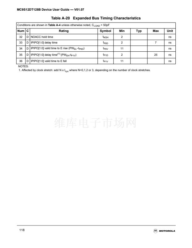
Table A-8 ATD Operating Characteristics
Conditions are shown in
Table A-4
unless otherwise noted
Num C
Reference Potential
1
2
3
4
D
Rating
Low
High
Symbol
V
RL
V
RH
V
RH
-V
RL
f
ATDCLK
Min
V
SSA
V
DDA
/2
4.50
0.5
14
7
12
6
Typ
Max
V
DDA
/2
V
DDA
Unit
V
V
V
MHz
Cycles
碌s
Cycles
碌s
碌s
mA
mA
C Differential Reference Voltage
1
D ATD Clock Frequency
ATD 10-Bit Conversion Period
D
5.00
5.25
2.0
28
14
26
13
20
0.75
0.375
Clock Cycles
2
N
CONV10
Conv, Time at 2.0MHz ATD Clock f
ATDCLK
T
CONV10
ATD 8-Bit Conversion Period
Clock Cycles
(2)
Conv, Time at 2.0MHz ATD Clock f
ATDCLK
5
D
N
CONV8
T
CONV8
t
SR
I
REF
I
REF
6
7
8
D Stop Recovery Time (V
DDA
=5.0 Volts)
P Reference Supply current (Both ATD modules on)
P Reference Supply current (Only one ATD module on)
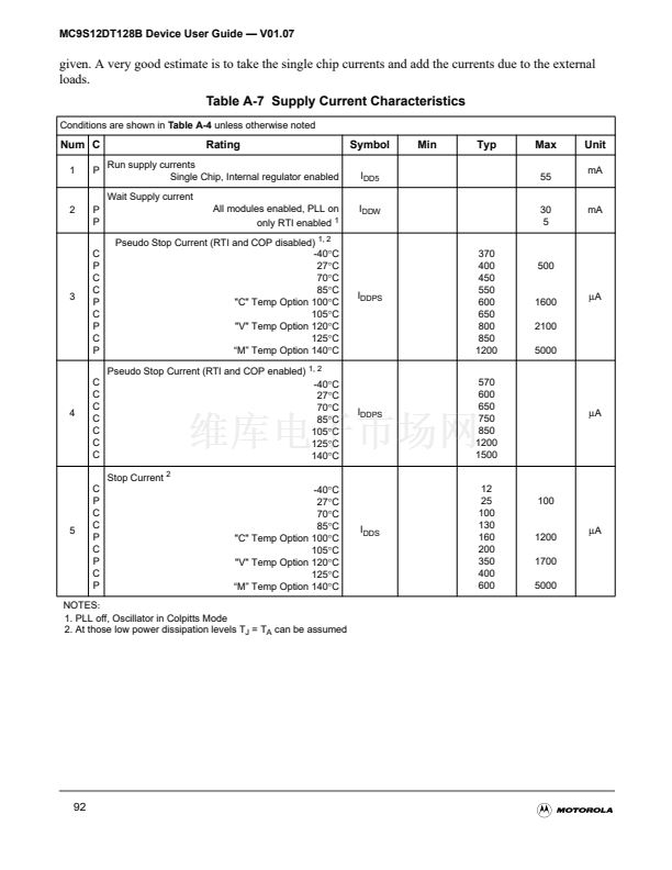
NOTES:
1. Full accuracy is not guaranteed when differential voltage is less than 4.50V
2. The minimum time assumes a final sample period of 2 ATD clocks cycles while the maximum time assumes a final sample
period of 16 ATD clocks.
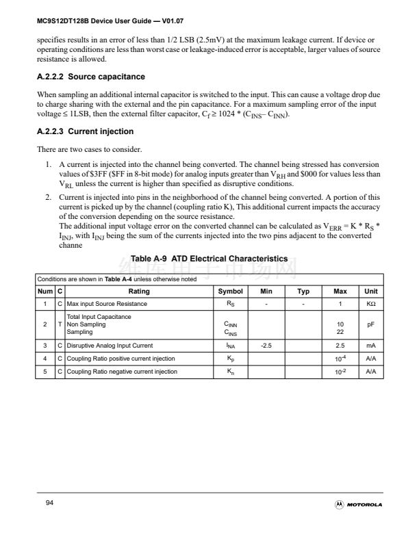
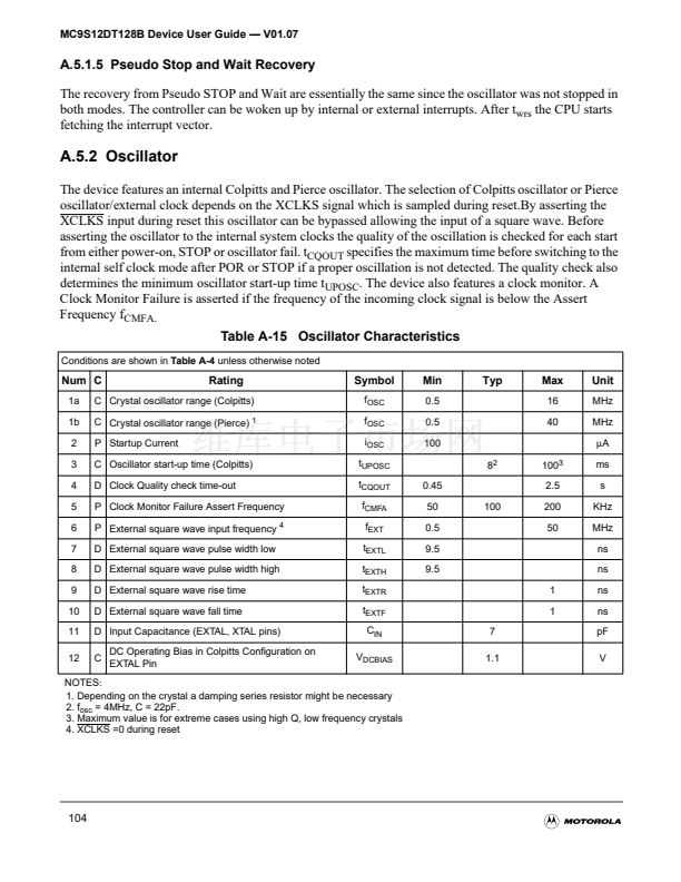
A.2.2 Factors influencing accuracy
Three factors 鈥?source resistance, source capacitance and current injection 鈥?have an influence on the
accuracy of the ATD.
A.2.2.1 Source Resistance:
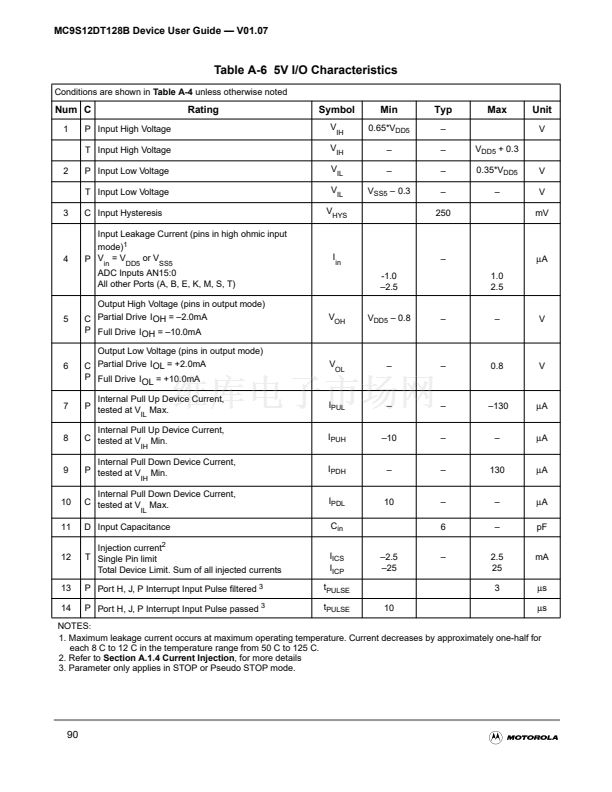
Due to the input pin leakage current as specified in
Table A-6
in conjunction with the source resistance
there will be a voltage drop from the signal source to the ATD input. The maximum source resistance R
S
93


 1
1
 2
2
 3
3
 4
4
 5
5
 6
6
 7
7
 8
8
 9
9
 10
10
 11
11
 12
12
 13
13
 14
14
 15
15
 16
16
 17
17
 18
18
 19
19
 20
20
 21
21
 22
22
 23
23
 24
24
 25
25
 26
26
 27
27
 28
28
 29
29
 30
30
 31
31
 32
32
 33
33
 34
34
 35
35
 36
36
 37
37
 38
38
 39
39
 40
40
 41
41
 42
42
 43
43
 44
44
 45
45
 46
46
 47
47
 48
48
 49
49
 50
50
 51
51
 52
52
 53
53
 54
54
 55
55
 56
56
 57
57
 58
58
 59
59
 60
60
 61
61
 62
62
 63
63
 64
64
 65
65
 66
66
 67
67
 68
68
 69
69
 70
70
 71
71
 72
72
 73
73
 74
74
 75
75
 76
76
 77
77
 78
78
 79
79
 80
80
 81
81
 82
82
 83
83
 84
84
 85
85
 86
86
 87
87
 88
88
 89
89
 90
90
 91
91
 92
92
 93
93
 94
94
 95
95
 96
96
 97
97
 98
98
 99
99
 100
100
 101
101
 102
102
 103
103
 104
104
 105
105
 106
106
 107
107
 108
108
 109
109
 110
110
 111
111
 112
112
 113
113
 114
114
 115
115
 116
116
 117
117
 118
118
 119
119
 120
120
 121
121
 122
122
 123
123
 124
124
