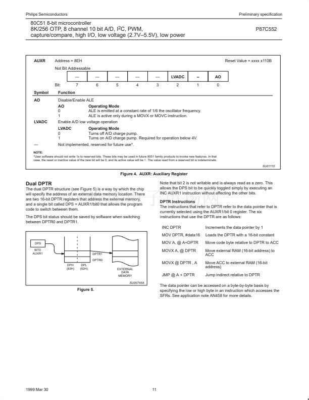
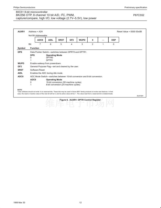
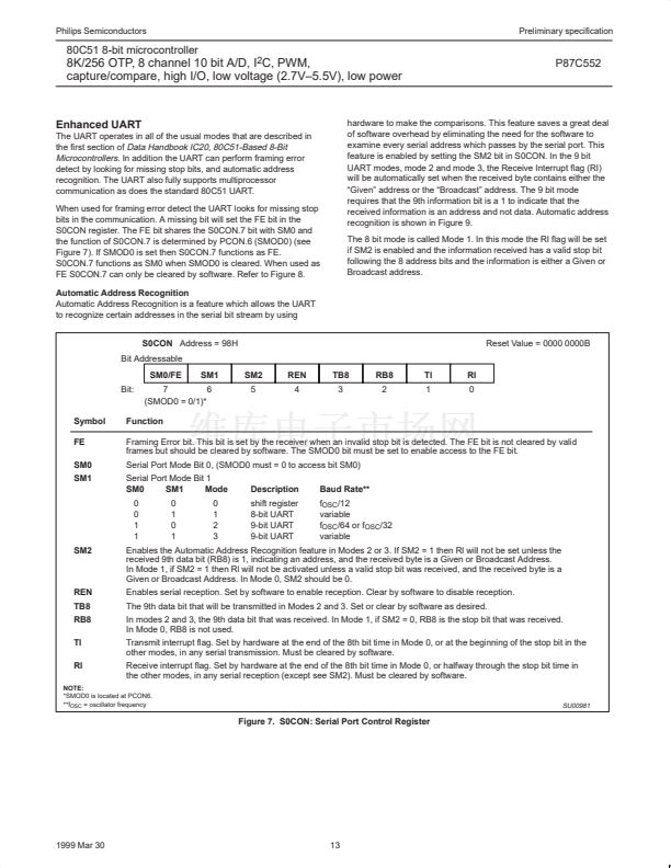
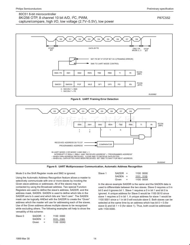
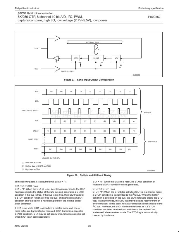
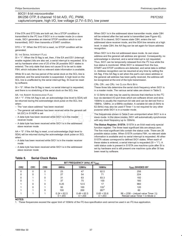
k鈩?/div>
pF
碌s
碌s
碌s
碌s
LSB
LSB
LSB
LSB
LSB
%
LSB
LSB
dB
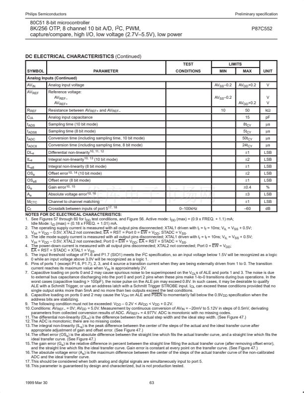
PARAMETER
CONDITIONS
MIN
LIMITS
MAX
UNIT
R
REF
C
IA
t
ADS
t
ADS8
t
ADC
t
ADC8
DL
e
IL
e
IL
e8
OS
e
OS
e8
G
e
A
e
M
CTC
C
t
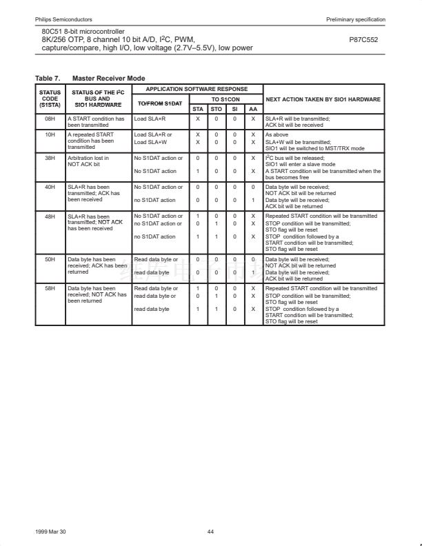
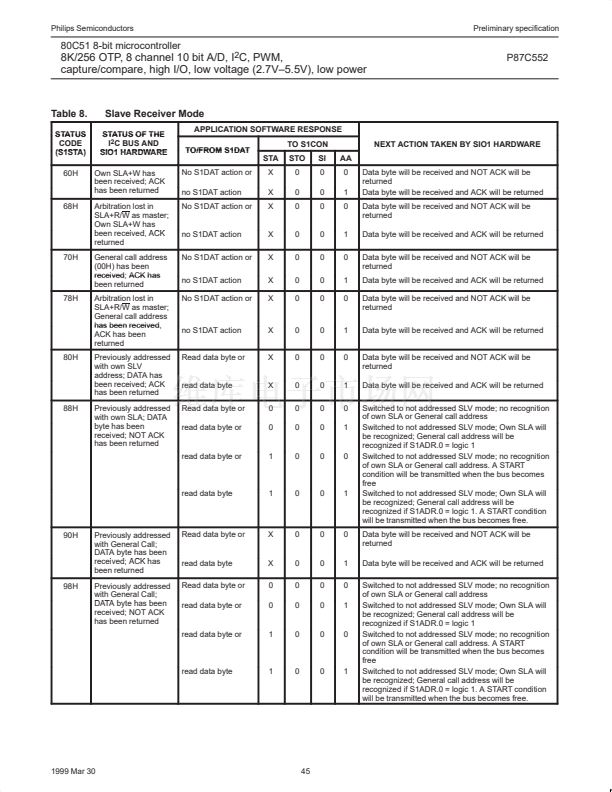
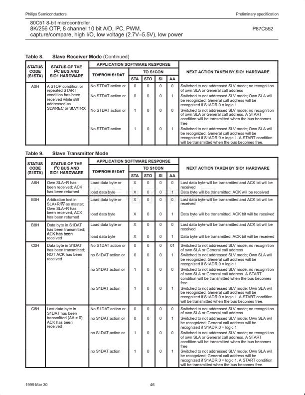
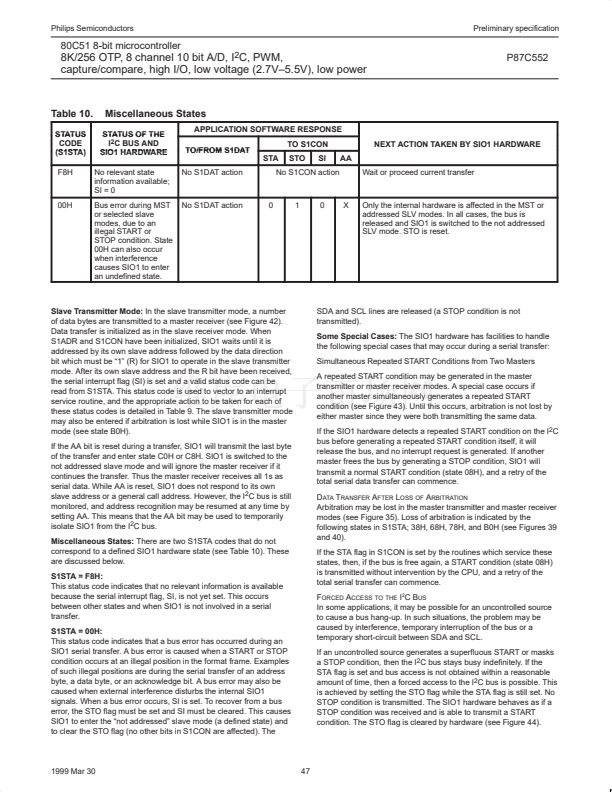
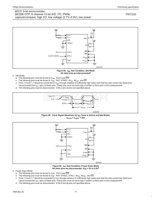
NOTES FOR DC ELECTRICAL CHARACTERISTICS:
1. See Figures 57 through 60 for I
DD
test conditions, and Figure 56. Active mode: I
DD
(max) = (0.9 x FREQ. + 1.1) mA;
Idle Mode: I
ID
(max) = (0.18 x FREQ. + 1.01) mA.
2. The operating supply current is measured with all output pins disconnected; XTAL1 driven with t
r
= t
f
= 10ns; V
IL
= V
SS
+ 0.5V;
V
IH
= V
DD
鈥?0.5V; XTAL2 not connected; EA = RST = Port 0 = EW = V
DD
; STADC = V
SS
.
3. The idle mode supply current is measured with all output pins disconnected; XTAL1 driven with t
r
= t
f
= 10ns; V
IL
= V
SS
+ 0.5V;
V
IH
= V
DD
鈥?0.5V; XTAL2 not connected; Port 0 = EW = V
DD
; EA = RST = STADC = V
SS
.
4. The power-down current is measured with all output pins disconnected; XTAL2 not connected; Port 0 = EW = V
DD
;
EA = RST = STADC = XTAL1 = V
SS
.
5. The input threshold voltage of P1.6 and P1.7 (SIO1) meets the I
2
C specification, so an input voltage below 1.5V will be recognized as a logic
0 while an input voltage above 3.0V will be recognized as a logic 1.
6. Pins of ports 1 (except P1.6, P1.7), 2, 3, and 4 source a transition current when they are being externally driven from 1 to 0. The transition
current reaches its maximum value when V
IN
is approximately 2V.
7. Capacitive loading on ports 0 and 2 may cause spurious noise to be superimposed on the V
OL
s of ALE and ports 1 and 3. The noise is due
to external bus capacitance discharging into the port 0 and port 2 pins when these pins make 1-to-0 transitions during bus operations. In the
worst cases (capacitive loading > 100pF), the noise pulse on the ALE pin may exceed 0.8V. In such cases, it may be desirable to qualify
ALE with a Schmitt Trigger, or use an address latch with a Schmitt Trigger STROBE input. I
OL
can exceed these conditions provided that no
single output sinks more than 5mA and no more than two outputs exceed the test conditions.
8. Capacitive loading on ports 0 and 2 may cause the V
OH
on ALE and PSEN to momentarily fall below the 0.9V
DD
specification when the
address bits are stabilizing.
9. The following condition must not be exceeded: V
DD
鈥?0.2V < AV
DD
< V
DD
+ 0.2V.
10. Conditions: AV
REF鈥?/div>
= 0V; AV
DD
= 5.0V. Measurement by continuous conversion of AV
IN
= 鈥?0mV to 5.12V in steps of 0.5mV, derivating
parameters from collected conversion results of ADC. AV
REF+
= 4.977V. ADC is monotonic with no missing codes.
11. The differential non-linearity (DL
e
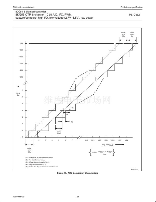
) is the difference between the actual step width and the ideal step width. (See Figure 47.)
12. The ADC is monotonic; there are no missing codes.
13. The integral non-linearity (IL
e
) is the peak difference between the center of the steps of the actual and the ideal transfer curve after
appropriate adjustment of gain and offset error. (See Figure 47.)
14. The offset error (OS
e
) is the absolute difference between the straight line which fits the actual transfer curve, and a straight line which fits the
ideal transfer curve. (See Figure 47.)
15. The gain error (G
e
) is the relative difference in percent between the straight line fitting the actual transfer curve (after removing offset error),
and the straight line which fits the ideal transfer curve. Gain error is constant at every point on the transfer curve. (See Figure 47.)
16. The absolute voltage error (A
e
) is the maximum difference between the center of the steps of the actual transfer curve of the non-calibrated
ADC and the ideal transfer curve.
17. This should be considered when both analog and digital signals are simultaneously input to port 5.
18. This parameter is guaranteed by design and characterized, but is not production tested.
1999 Mar 30
63


 1
1
 2
2
 3
3
 4
4
 5
5
 6
6
 7
7
 8
8
 9
9
 10
10
 11
11
 12
12
 13
13
 14
14
 15
15
 16
16
 17
17
 18
18
 19
19
 20
20
 21
21
 22
22
 23
23
 24
24
 25
25
 26
26
 27
27
 28
28
 29
29
 30
30
 31
31
 32
32
 33
33
 34
34
 35
35
 36
36
 37
37
 38
38
 39
39
 40
40
 41
41
 42
42
 43
43
 44
44
 45
45
 46
46
 47
47
 48
48
 49
49
 50
50
 51
51
 52
52
 53
53
 54
54
 55
55
 56
56
 57
57
 58
58
 59
59
 60
60
 61
61
 62
62
 63
63
 64
64
 65
65
 66
66
 67
67
 68
68
 69
69
 70
70
 71
71
 72
72
 73
73
 74
74
