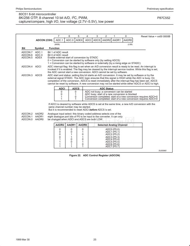
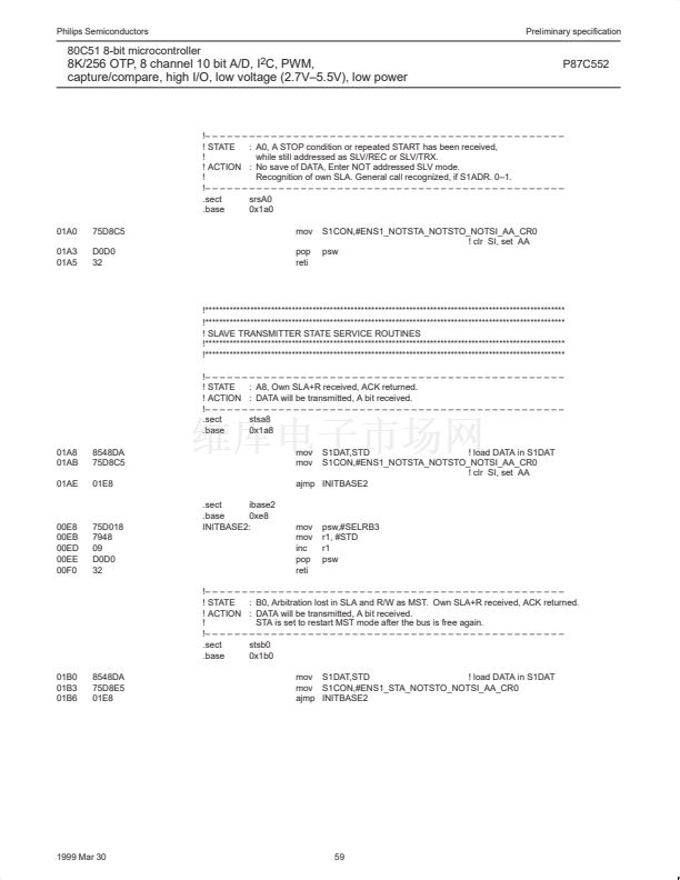
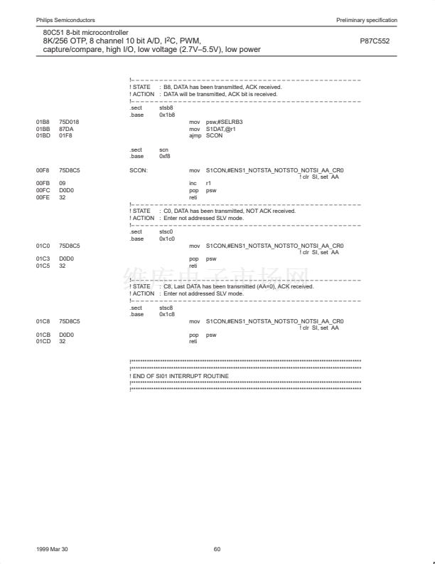
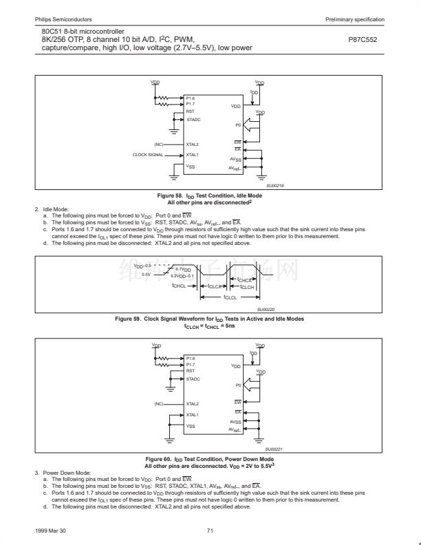
Figure 58. I
2. Idle Mode:
a. The following pins must be forced to V
: Port 0 and EW.
b. The following pins must be forced to V
ref鈥?/div>
, and EA.
c. Ports 1.6 and 1.7 should be connected to V
DD
through resistors of sufficiently high value such that the sink current into these pins
cannot exceed the I
OL1
spec of these pins. These pins must not have logic 0 written to them prior to this measurement.
d. The following pins must be disconnected: XTAL2 and all pins not specified above.
V
DD
鈥?.5
0.5V
0.7V
DD
0.2V
DD
鈥?.1
t
CHCL
t
CLCX
t
CLCL
t
CHCX
t
CLCH
SU00220
Figure 59. Clock Signal Waveform for I
DD
Tests in Active and Idle Modes
t
CLCH
= t
CHCL
= 5ns
V
DD
P1.6
P1.7
RST
STADC
P0
V
DD
I
DD
V
DD
V
DD
(NC)
XTAL2
XTAL1
V
SS
EW
EA
AV
SS
AV
ref鈥?/div>
SU00221
Figure 60. I
DD
Test Condition, Power Down Mode
All other pins are disconnected. V
DD
= 2V to 5.5V
3
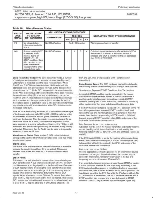
3. Power Down Mode:
a. The following pins must be forced to V
DD
: Port 0 and EW.
b. The following pins must be forced to V
SS
: RST, STADC, XTAL1, AV
ss
, AV
ref鈥?/div>
, and EA.
c. Ports 1.6 and 1.7 should be connected to V
DD
through resistors of sufficiently high value such that the sink current into these pins
cannot exceed the I
OL1
spec of these pins. These pins must not have logic 0 written to them prior to this measurement.
d. The following pins must be disconnected: XTAL2 and all pins not specified above.
1999 Mar 30
71


 1
1
 2
2
 3
3
 4
4
 5
5
 6
6
 7
7
 8
8
 9
9
 10
10
 11
11
 12
12
 13
13
 14
14
 15
15
 16
16
 17
17
 18
18
 19
19
 20
20
 21
21
 22
22
 23
23
 24
24
 25
25
 26
26
 27
27
 28
28
 29
29
 30
30
 31
31
 32
32
 33
33
 34
34
 35
35
 36
36
 37
37
 38
38
 39
39
 40
40
 41
41
 42
42
 43
43
 44
44
 45
45
 46
46
 47
47
 48
48
 49
49
 50
50
 51
51
 52
52
 53
53
 54
54
 55
55
 56
56
 57
57
 58
58
 59
59
 60
60
 61
61
 62
62
 63
63
 64
64
 65
65
 66
66
 67
67
 68
68
 69
69
 70
70
 71
71
 72
72
 73
73
 74
74
