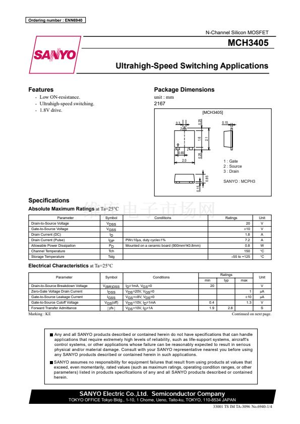
铮?/div>
y
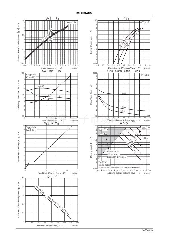
fs铮?-- ID
VDS=10V
掳
C
25
10
7
5
3
2
1.0
7
5
3
2
0.1
7
5
3
2
0.01
0.2
0.3
0.4
0.5
IF -- VSD
VGS=0
0.6
Ta=
75
掳
C
25
掳
C
--25
掳
C
0.7
0.8
0.9
C
5
掳
--2
掳
C
=
75
Ta
Forward Current, IF -- A
1.0
1.1
1.2
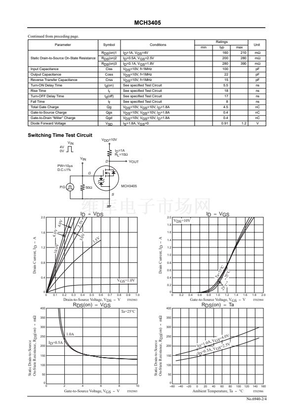
Drain Current, ID -- A
100
7
SW Time -- ID
VDD=10V
VGS=4V
1000
7
5
Ciss, Coss, Crss -- VDS
f=1MHz
Diode Forward Voltage, VSD -- V
IT02988
Switching Time, SW Time -- ns
5
3
2
td(off)
Ciss, Coss, Crss -- pF
3
2
tr
10
7
5
3
2
tf
td(on)
100
7
5
3
2
Ciss
Coss
Crss
0
2
4
6
8
10
12
14
16
18
20
1.0
0.1
10
2
3
5
7
1.0
2
3
5
IT02989
10
7
5
3
2
Drain Current, ID -- A
10
9
Drain-to-Source Voltage, VDS -- V
IT02990
VGS -- Qg
ASO
Gate-to-Source Voltage, VGS -- V
VDS=10V
ID=1.8A
IDP=7.2A
<10碌s
1m
8
ID=1.8A
s
Drain Current, ID -- A
10
7
6
5
4
3
2
1
0
0
1
2
3
4
5
IT02991
m
1.0
7
5
3
2
0.1
7
5
3
2
s
100碌s
10
n
s
tio
0m
pera
o
DC
Operation in
this area is
limited by RDS(on).
0.01
0.01
Ta=25掳C
Single pulse
Mounted on a ceramic board (900mm
2
!0.8mm)
2 3
5 7 0.1
2 3
5 7 1.0
2 3
5 7 10
2 3
Total Gate Charge, Qg -- nC
1.0
Drain-to-Source Voltage, VDS -- V
5 7 100
IT02992
PD -- Ta
M
Allowable Power Dissipation, PD -- W
0.8
ou
nt
ed
on
0.6
ac
er
am
ic
b
oa
rd
0.4
(9
00
m
m
2
!
0
0.2
.8m
m
)
0
0
20
40
60
80
100
120
140
160
Amibient Tamperature, Ta --
掳C
IT02993
No.6940-3/4


 1
1
 2
2
 3
3
 4
4
