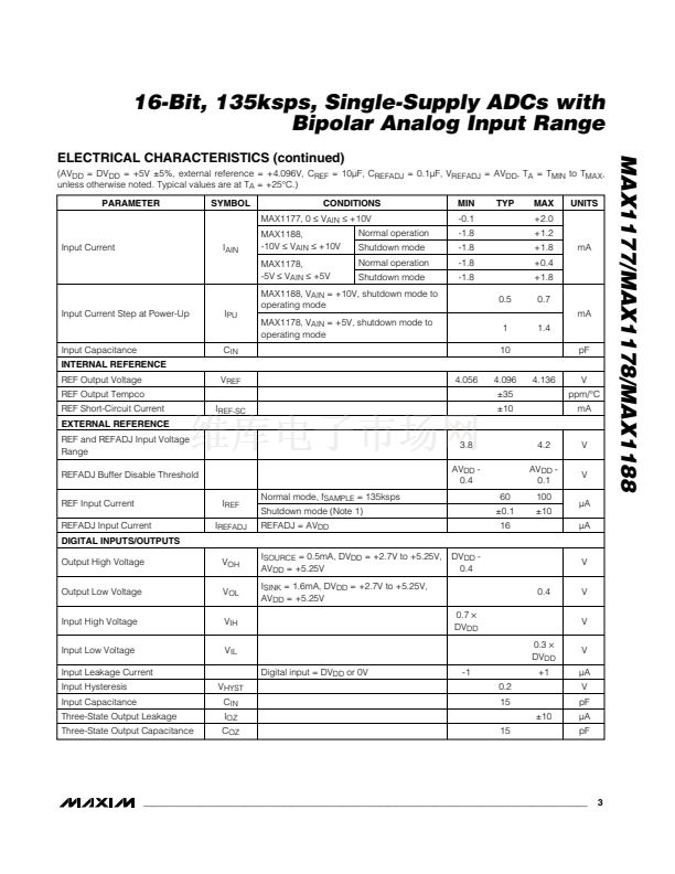
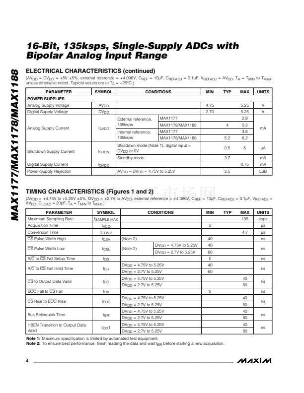
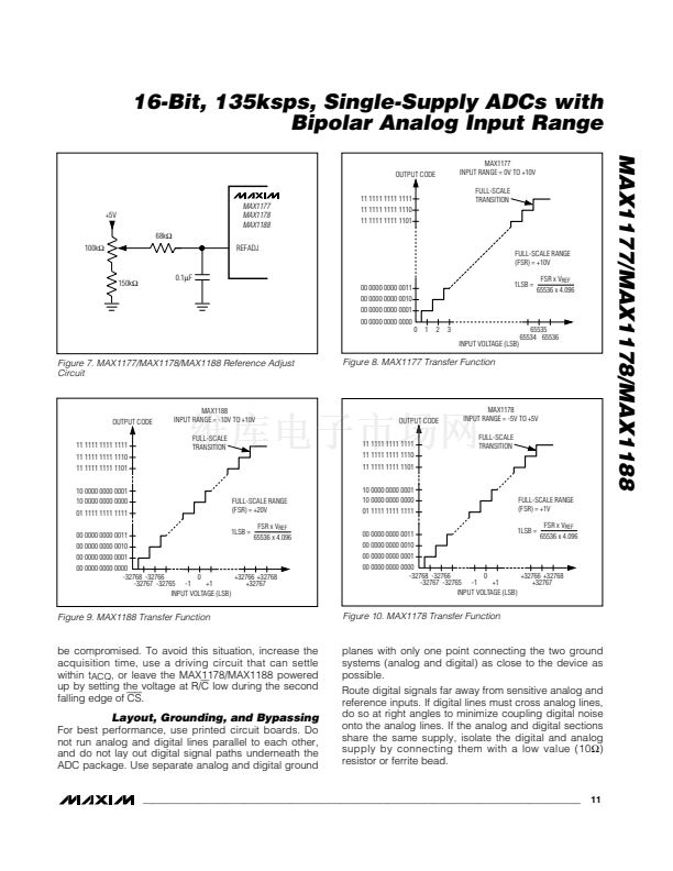
150k鈩?/div>
0.1碌F
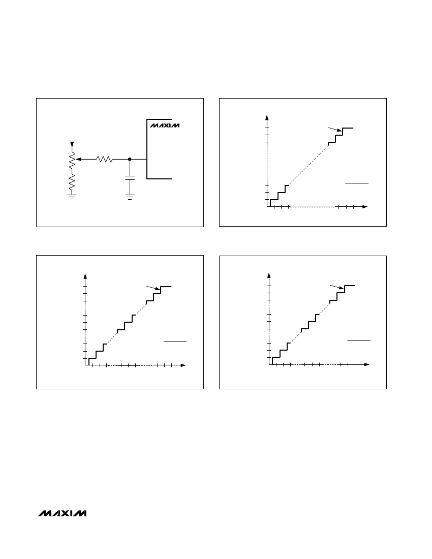
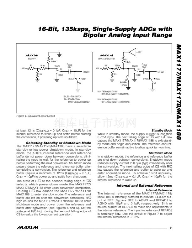
Figure 7. MAX1177/MAX1178/MAX1188 Reference Adjust
Circuit
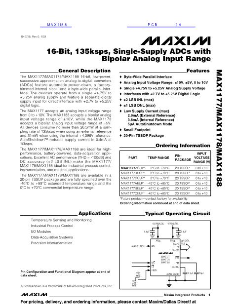
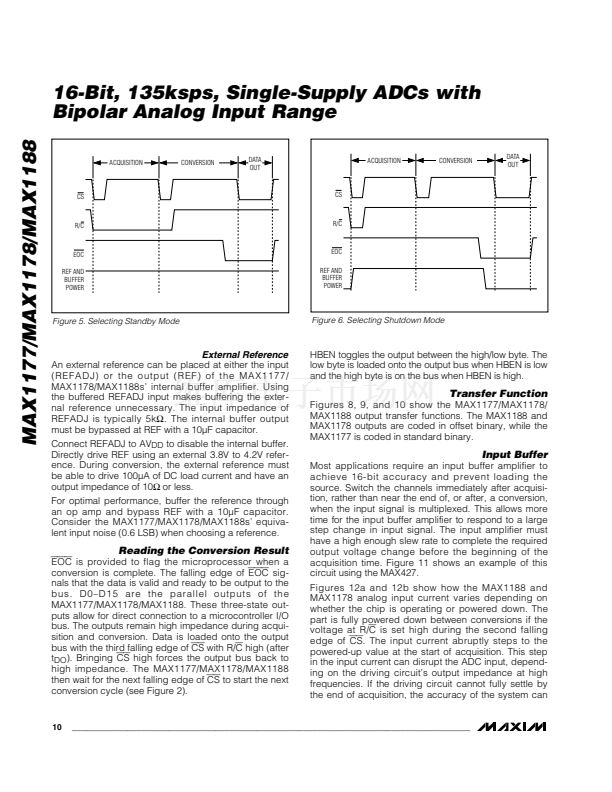
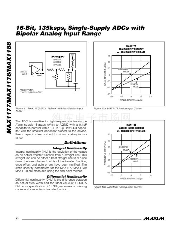
Figure 8. MAX1177 Transfer Function
OUTPUT CODE
11 1111 1111 1111
11 1111 1111 1110
11 1111 1111 1101
10 0000 0000 0001
10 0000 0000 0000
01 1111 1111 1111
00 0000 0000 0011
00 0000 0000 0010
00 0000 0000 0001
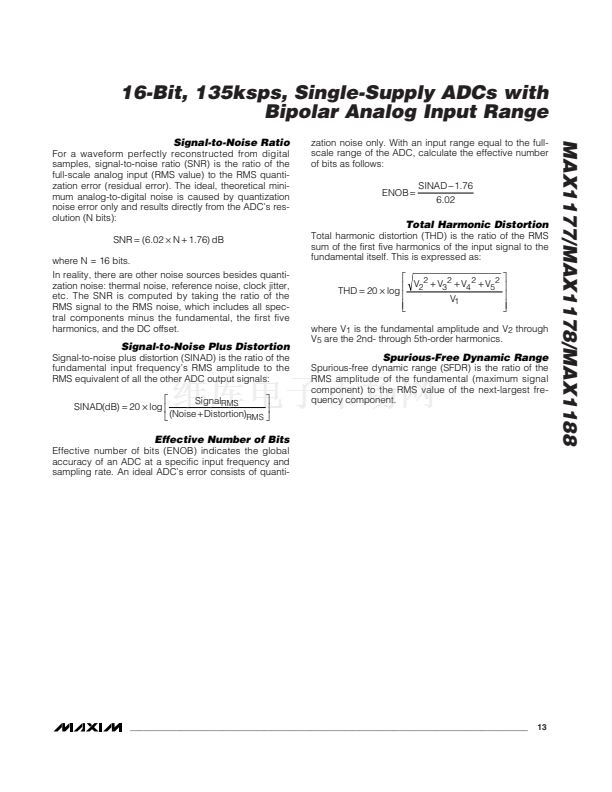
MAX1188
INPUT RANGE = -10V TO +10V
FULL-SCALE
TRANSITION
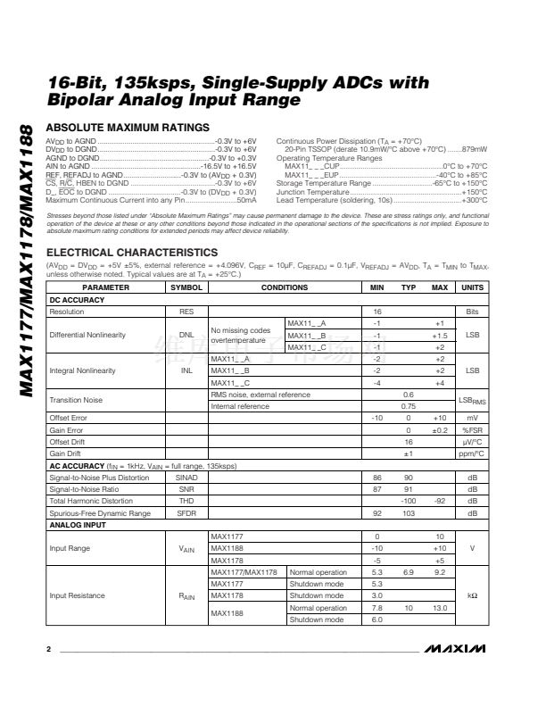
OUTPUT CODE
11 1111 1111 1111
11 1111 1111 1110
11 1111 1111 1101
10 0000 0000 0001
10 0000 0000 0000
01 1111 1111 1111
00 0000 0000 0011
00 0000 0000 0010
00 0000 0000 0001
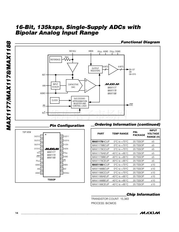
MAX1178
INPUT RANGE = -5V TO +5V
FULL-SCALE
TRANSITION
FULL-SCALE RANGE
(FSR) = +20V
1LSB =
FSR x V
REF
65536 x 4.096
FULL-SCALE RANGE
(FSR) = +1V
1LSB =
FSR x V
REF
65536 x 4.096
00 0000 0000 0000
0
+32766 +32768
-32768 -32766
+1
-32767 -32765 -1
+32767
INPUT VOLTAGE (LSB)
00 0000 0000 0000
0
+32766 +32768
-32768 -32766
+1
-32767 -32765 -1
+32767
INPUT VOLTAGE (LSB)
Figure 9. MAX1188 Transfer Function
Figure 10. MAX1178 Transfer Function
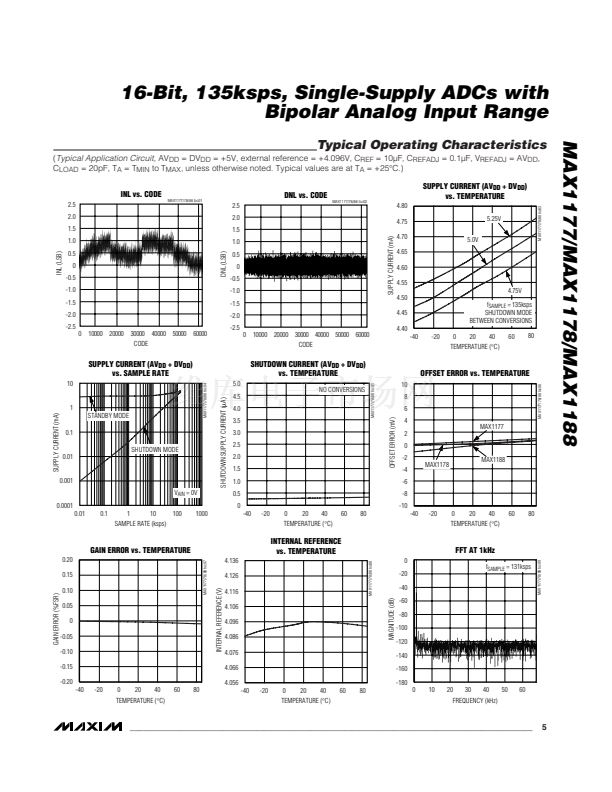
be compromised. To avoid this situation, increase the
acquisition time, use a driving circuit that can settle
within t
ACQ
, or leave the MAX1178/MAX1188 powered
up by setting the voltage at R/C low during the second
falling edge of
CS.
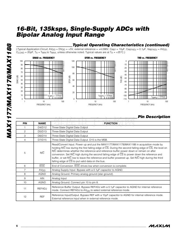
Layout, Grounding, and Bypassing
For best performance, use printed circuit boards. Do
not run analog and digital lines parallel to each other,
and do not lay out digital signal paths underneath the
ADC package. Use separate analog and digital ground
planes with only one point connecting the two ground
systems (analog and digital) as close to the device as
possible.
Route digital signals far away from sensitive analog and
reference inputs. If digital lines must cross analog lines,
do so at right angles to minimize coupling digital noise
onto the analog lines. If the analog and digital sections
share the same supply, isolate the digital and analog
supply by connecting them with a low value (10鈩?
resistor or ferrite bead.
______________________________________________________________________________________
11


 1
1
 2
2
 3
3
 4
4
 5
5
 6
6
 7
7
 8
8
 9
9
 10
10
 11
11
 12
12
 13
13
 14
14
 15
15
