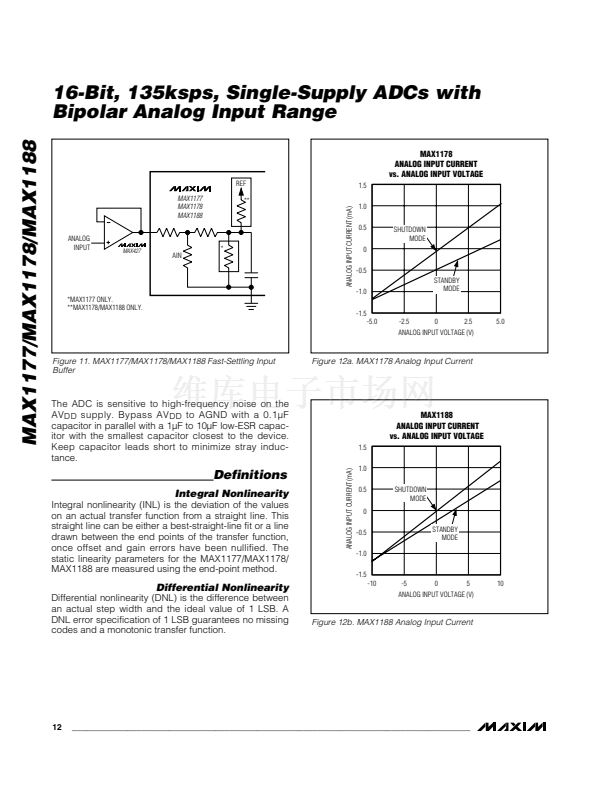
16-Bit, 135ksps, Single-Supply ADCs with
Bipolar Analog Input Range
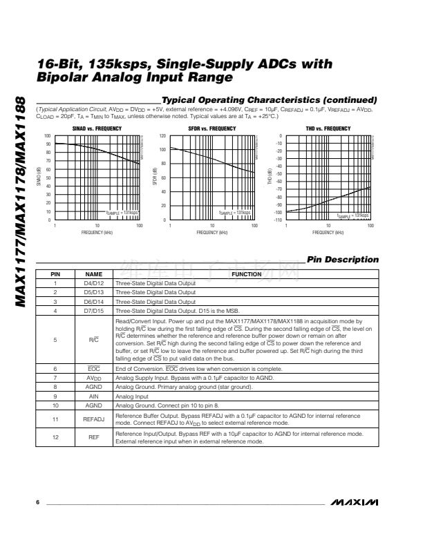
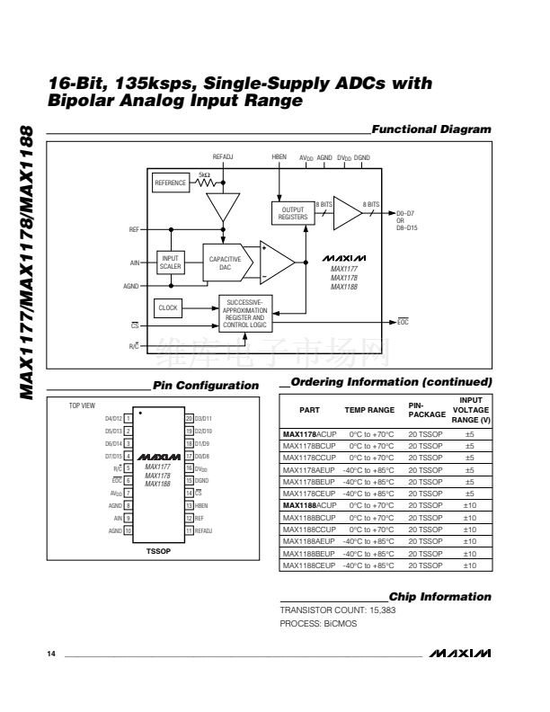
Pin Description (continued)
PIN
13
NAME
HBEN
FUNCTION
High-Byte Enable Input. Used to multiplex the 16-bit conversion result.
1: Most significant byte available on the data bus.
0: Least significant byte available on the data bus.
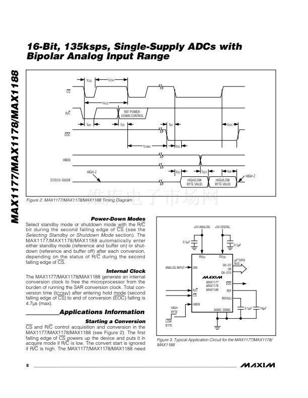
Convert Start. The first falling edge of
CS
powers up the device and enables acquire mode when R/C
is low. The second falling edge of
CS
starts conversion. The third falling edge of
CS
loads the result
onto the bus when R/C is high.
Digital Ground
Digital Supply Voltage. Bypass with a 0.1碌F capacitor to DGND.
Three-State Digital Data Output. D0 is the LSB.
Three-State Digital Data Output
Three-State Digital Data Output
Three-State Digital Data Output
MAX1177/MAX1178/MAX1188
14
15
16
17
18
19
20
CS
DGND
DV
DD
D0/D8
D1/D9
D2/D10
D3/D11
DV
DD
1mA
DO鈥揇15
DO鈥揇15
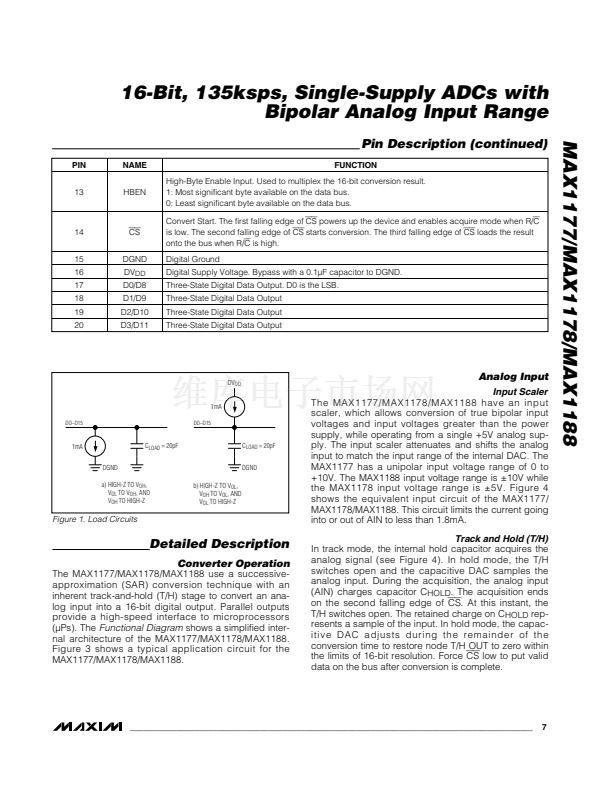
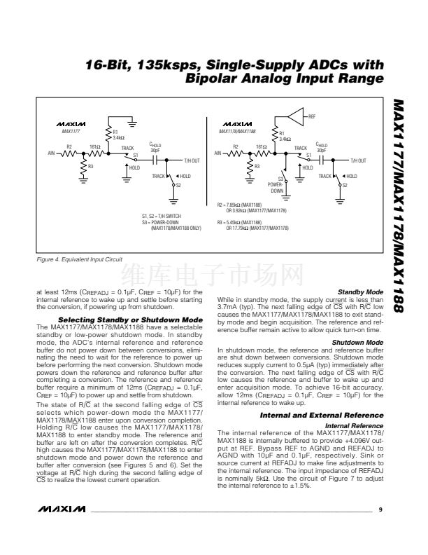
Analog Input
Input Scaler
The MAX1177/MAX1178/MAX1188 have an input
scaler, which allows conversion of true bipolar input
voltages and input voltages greater than the power
supply, while operating from a single +5V analog sup-
ply. The input scaler attenuates and shifts the analog
input to match the input range of the internal DAC. The
MAX1177 has a unipolar input voltage range of 0 to
+10V. The MAX1188 input voltage range is 卤10V while
the MAX1178 input voltage range is 卤5V. Figure 4
shows the equivalent input circuit of the MAX1177/
MAX1178/MAX1188. This circuit limits the current going
into or out of AIN to less than 1.8mA.
Track and Hold (T/H)
In track mode, the internal hold capacitor acquires the
analog signal (see Figure 4). In hold mode, the T/H
switches open and the capacitive DAC samples the
analog input. During the acquisition, the analog input
(AIN) charges capacitor C
HOLD
. The acquisition ends
on the second falling edge of
CS.
At this instant, the
T/H switches open. The retained charge on C
HOLD
rep-
resents a sample of the input. In hold mode, the capac-
itive DAC adjusts during the remainder of the
conversion time to restore node T/H OUT to zero within
the limits of 16-bit resolution. Force
CS
low to put valid
data on the bus after conversion is complete.
1mA
DGND
C
LOAD
= 20pF
C
LOAD
= 20pF
DGND
b) HIGH-Z TO V
OL
,
V
OH
TO V
OL
, AND
V
OL
TO HIGH-Z
a) HIGH-Z TO V
OH
,
V
OL
TO V
OH
, AND
V
OH
TO HIGH-Z
Figure 1. Load Circuits
Detailed Description
Converter Operation
The MAX1177/MAX1178/MAX1188 use a successive-
approximation (SAR) conversion technique with an
inherent track-and-hold (T/H) stage to convert an ana-
log input into a 16-bit digital output. Parallel outputs
provide a high-speed interface to microprocessors
(碌Ps). The
Functional Diagram
shows a simplified inter-
nal architecture of the MAX1177/MAX1178/MAX1188.
Figure 3 shows a typical application circuit for the
MAX1177/MAX1178/MAX1188.
_______________________________________________________________________________________
7


 1
1
 2
2
 3
3
 4
4
 5
5
 6
6
 7
7
 8
8
 9
9
 10
10
 11
11
 12
12
 13
13
 14
14
 15
15
