MM74HC4046
Detailed Circuit Description
VOLTAGE CONTROLLED OSCILLATOR/SOURCE
FOLLOWER
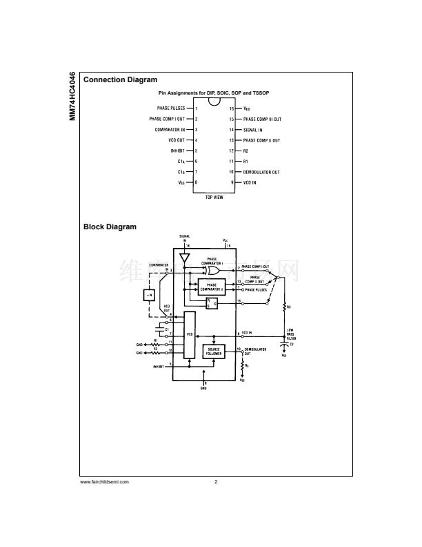
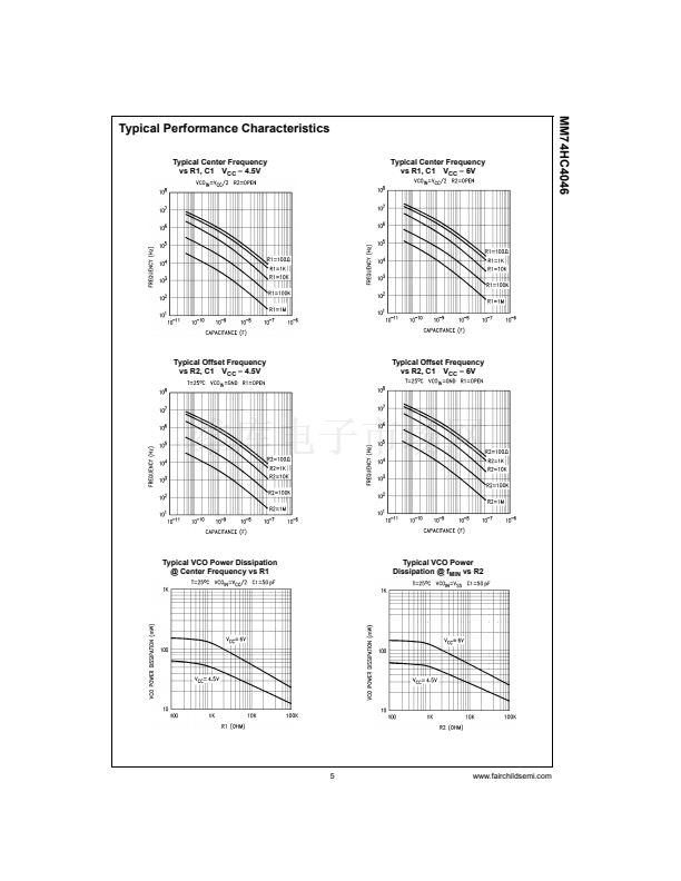
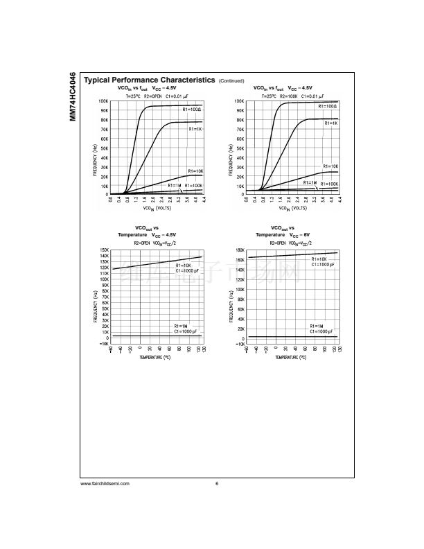
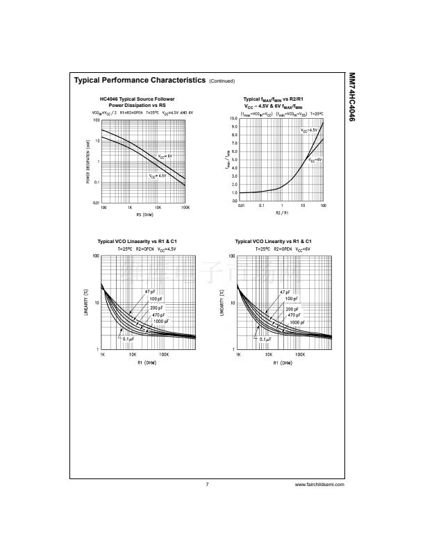
The VCO requires two or three external components to
operate. These are R1, R2, C1. Resistor R1 and capacitor
C1 are selected to determine the center frequency of the
VCO. R1 controls the lock range. As R1鈥檚 resistance
decreases the range of f
MIN
to f
MAX
increases. Thus the
VCO鈥檚 gain increases. As C1 is changed the offset (if used)
of R2, and the center frequency is changed. (See typical
performance curves) R2 can be used to set the offset fre-
quency with 0V at VCO input. If R2 is omitted the VCO
range is from 0Hz. As R2 is decreased the offset frequency
is increased. The effect of R2 is shown in the design infor-
mation table and typical performance curves. By increasing
the value of R2 the lock range of the PLL is offset above
0Hz and the gain (Hz/Volt) does not change. In general,
when offset is desired, R2 and C1 should be chosen first,
and then R1 should be chosen to obtain the proper center
frequency.
Internally the resistors set a current in a current mirror as
shown in Figure 1. The mirrored current drives one side of
the capacitor once the capacitor charges up to the thresh-
old of the schmitt trigger the oscillator logic flips the capaci-
tor over and causes the mirror to charge the opposite side
of the capacitor. The output from the internal logic is then
taken to pin 4.
VCO WITHOUT OFFSET
R2 =
鈭?/div>
VCO WITH OFFSET
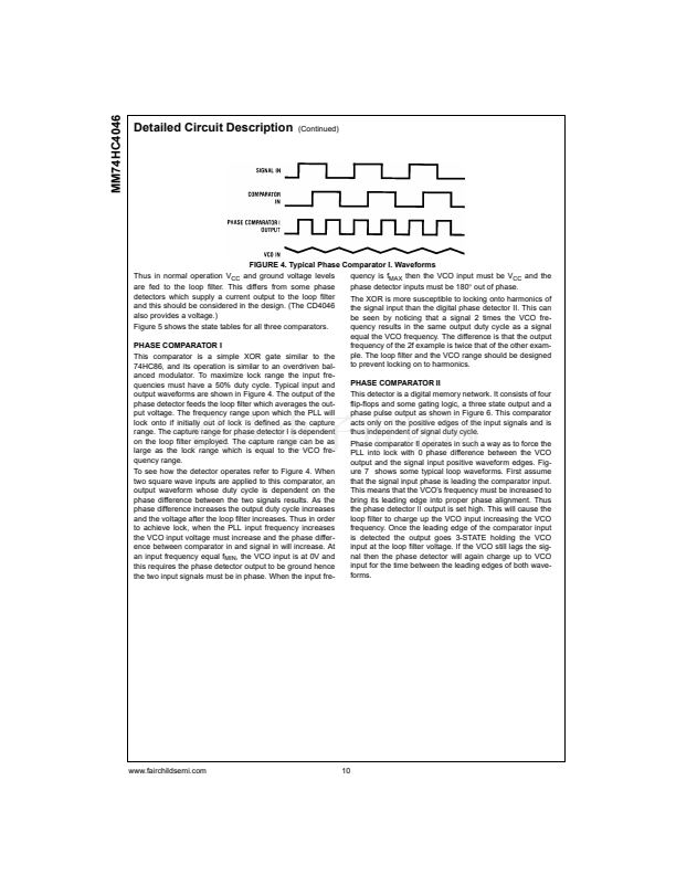
Comparator I
R
2
= 鈭?/div>
鈥iven: f
0
鈥se f
0
with curve titled
center frequency vs R1, C
to determine R1 and C1
R
2
鈮犫垶
鈥iven: f
0
and f
L
鈥alculate f
MIN
from the
equation f
MIN
=
f
o
鈭?/div>
f
L
鈥se f
MIN
with curve titled
offset frequency vs R2, C
to determine R2 and C1
鈥alculate f
MAX
/f
MIN
from
the equation f
MAX
/f
MIN
=
f
o
+
f
L
/f
o
鈭?/div>
f
L
鈥se f
MAX
/f
MIN
with curve
titled f
MAX
/f
MIN
vs R2/R1
to determine ratio R2/R1
to obtain R1
FIGURE 1.
R
2
= 鈭?/div>
鈥iven: f
MAX
Comparator II & III
R
2
鈮犫垶
鈥iven: f
MIN
and f
MAX
鈥se f
MIN
with curve titled
offset frequency vs R2,
C to determine R2 and C1
鈥alculate f
MAX
/f
MIN
鈥se f
MAX
/f
MIN
with curve
titled f
MAX
/f
MIN
vs R2/R1
to determine ratio R2/R1
to obtain R1
鈥alculate f
0
from the
equation f
o
=
f
MAX
/2
鈥se f
0
with curve titled
center frequency vs R1, C
to determine R1 and C1
www.fairchildsemi.com
8
MM74HC4046 PDF文件相关型号
MM74HC4046
MM74HC4046相关型号PDF文件下载
-
型号
版本
描述
厂商
下载
-
英文版
National Semiconductor [Synchronous Decade Counter with Asy...
NSC
-
英文版
Quad 2-Input NAND Gate, Quad 2-Input NOR Gate, Hex Inverter,...
NSC
-
英文版
Quad 2-Input NAND Gate . Quad 2-Input NOR Gate . Hex Inverte...
FAIRCHILD
-
英文版
Quad 2-Input NAND Gate . Quad 2-Input NOR Gate . Hex Inverte...
FAIRCHILD ...
-
英文版
Quad 2-Input NAND Gate, Quad 2-Input NOR Gate, Hex Inverter,...
NSC [Natio...
-
英文版
Quad 2-Input NAND Gate . Quad 2-Input NOR Gate . Hex Inverte...
FAIRCHILD
-
英文版
Quad 2-Input NAND Gate, Quad 2-Input NOR Gate, Hex Inverter,...
NSC
-
英文版
Quad 2-Input NAND Gate, Quad 2-Input NOR Gate, Hex Inverter,...
NSC [Natio...
-
英文版
Quad 2-Input NAND Gate . Quad 2-Input NOR Gate . Hex Inverte...
FAIRCHILD ...
-
英文版
Quad 2-Input NAND Gate . Quad 2-Input NOR Gate . Hex Inverte...
FAIRCHILD
-
英文版
Quad 2-Input NAND Gate, Quad 2-Input NOR Gate, Hex Inverter,...
NSC
-
英文版
Quad 2-Input NAND Gate, Quad 2-Input NOR Gate, Hex Inverter,...
NSC [Natio...
-
英文版
Quad 2-Input NAND Gate . Quad 2-Input NOR Gate . Hex Inverte...
FAIRCHILD ...
-
英文版
Quad 2-Input AND Gate
FAIRCHILD
-
英文版
Quad 2-Input AND Gate
NSC
-
英文版
Quad 2-Input AND Gate
NSC [Natio...
-
英文版
Quad 2-Input AND Gate
FAIRCHILD ...
-
英文版
Quad 2-Input NAND Gate, Quad 2-Input NOR Gate, Hex Inverter,...
NSC
-
英文版
Quad 2-Input NAND Gate, Quad 2-Input NOR Gate, Hex Inverter,...
NSC [Natio...
-
英文版
Hex Schmitt Trigger
NSC


 1
1
 2
2
 3
3
 4
4
 5
5
 6
6
 7
7
 8
8
 9
9
 10
10
 11
11
 12
12
 13
13
 14
14
 15
15
 16
16
 17
17
