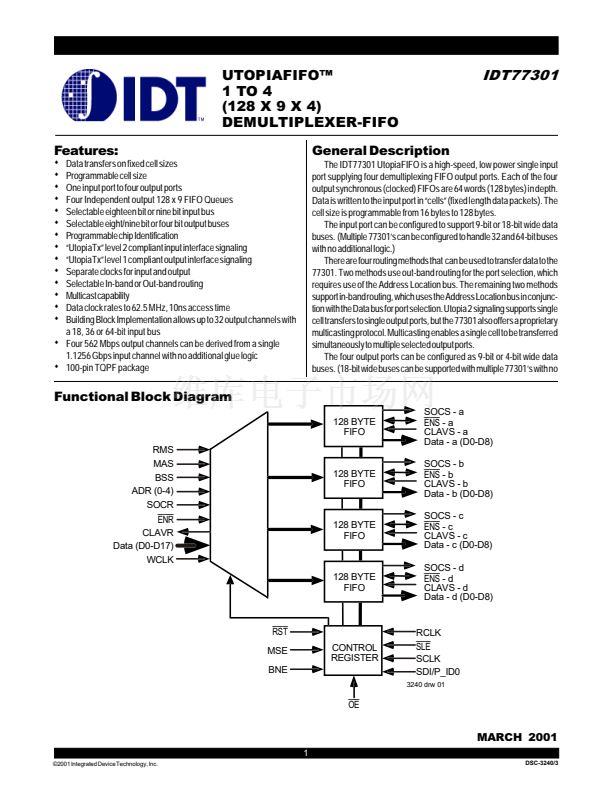
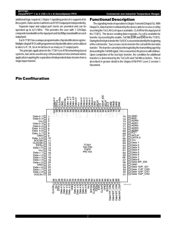
IDT77301
UtopiaFIFO鈩?1 to 4 (128 x 9 x 4) Demultiplexer-FIFO
Commercial and Industrial Temperature Ranges
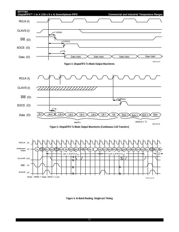
transferred,
ENS
is asserted, data is placed on the bus and SOCS is set
HIGH for the first 9-bit word transfer.
ENS
will remain LOW and data
transfer will continue until the entire cell is sent (see Figure 4). If during cell
transfer, CLAVS de-asserts, transfer continues. Continuous cell transfer
with no latency is possible. If CLAVS asserts prior to the last 9-bit word
transfer, and a complete cell can be sent,
ENS
remains LOW and the next
cell is sent. SOCS will assert during the first word transfer (see Figure 5).
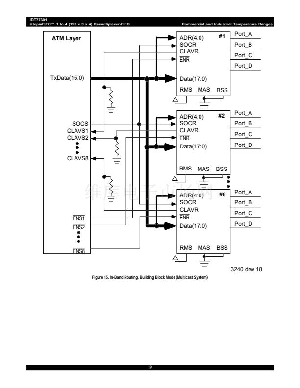
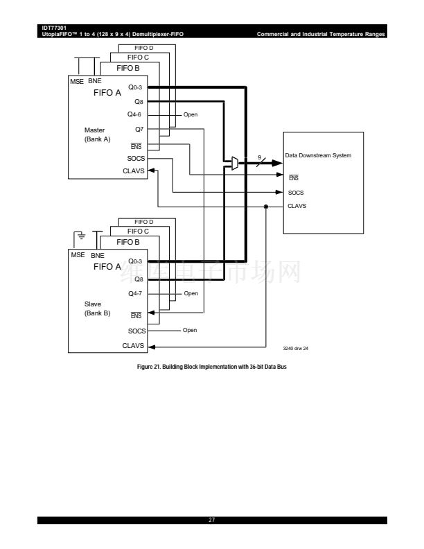
Three additional control signals provide added device functionality.
The global reset (RST) pin clears all register values. The Master Slave
Enable (MSE) and Byte Nibble Enable (BNE) pins are used in the building
block implementation with an input bus of 32 or 64-bits where up to 32
separate UtopiaFIFOs can be utilized. These pins allow the elimination of
glue logic in the building block mode and ensure synchronization of cells
on the output data bus.
The following sections describe in detail the input side timing and data/
signal connections for various combinations. The first four sections
describe operations for a single UtopiaFIFO implementation: In-Band
Routing-Single and Multicast; Out-Band Routing-Single and Multicast.
The next four sections describe usage in a building block implementation
(up to eight independent devices): In-Band Routing-Single and Multicast;
Out-Band Routing-Single and Multicast. A final section describes opera-
tions for a 36-bit input bus connected to a maximum of 16 UtopiaFIFOs.
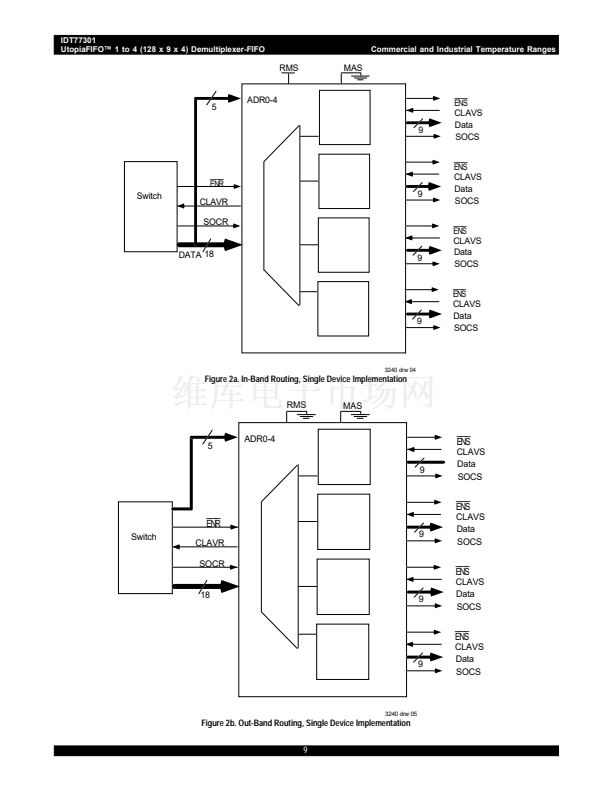
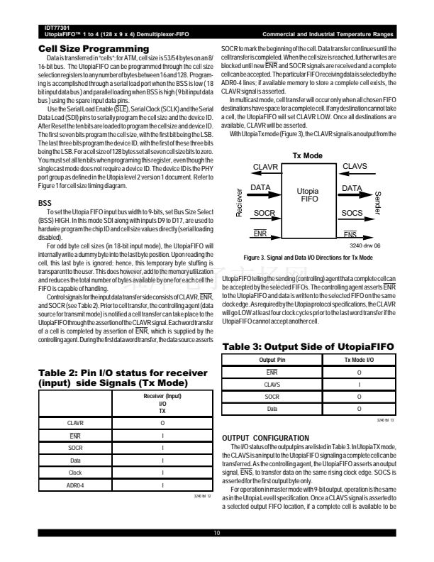
Single Device Implementation
IN-BAND ROUTING
SINGLE FIFO DESTINATION (NO MULTICAST)
Single FIFO destination timing is described by Figure 6. Figure 2a
shows the data/signal connections.
Configuration:
RMS = 鈥?鈥?indicates in-band routing.
MAS = 鈥?鈥?indicates singlecast mode.
BSS = 鈥淴鈥?either 9 or 18 bit operation
With no current cell transfer, CLAVR and SOCR are LOW, the
C
1
C
2
C
3
C
4
C
5
C
6
C
7
WCLK (I)
Address/
(I)
data
A
1
A
2
A
3
A
4
A
3
H
1
H
2
H
3
CLAVR (O)
C
1
C
2
C
3
C
4
WCLK (I)
Address/ (I)
data
ENR
(I)
A
1
H
1
A
n
H
1
H
2
H
3
H
4
SOCR (I)
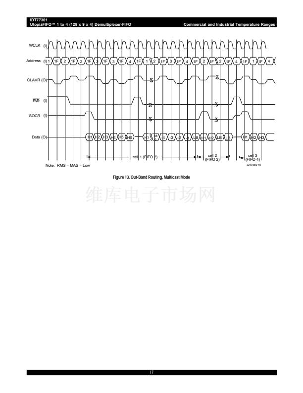
Note: RMS = High, MAS = Low
3240 drw 11
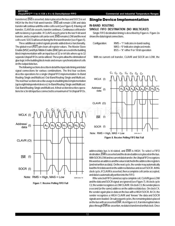
Figure 8. Receive Polling FIFO Not Full
CLAVR (O)
address/data bus is tri-stated, and
ENR
is HIGH. To select a FIFO
destination,
ENR
is asserted and the desired address is placed on the bus.
With SOCR LOW and no current data transfer, the UtopiaFIFO recognizes
this word as an address and the value is latched in the address line registers
(and not written as data). On the next cycle, the sender may automatically
load the first data word on the address/data bus and assert SOCR. At this
clock cycle, if CLAVR is asserted, then a complete cell can be accepted,
and data is automatically written into the FIFO.
If the selected FIFO cannot accept a complete cell, CLAVR goes LOW
and the data and SOCR signal are ignored (see Figure 7). At clock cycle
C2, the sender recognizes a LOW CLAVR. On clock C3, the sender places
a second (or the same) address on the address/data bus. On clock C4,
the sender again places data on the bus with a HIGH SOCR. At C4, the
sender recognizes a HIGH CLAVR and 鈥渒nows鈥?the data and SOCR
signals were loaded. On subsequent cycles, the remaining data is placed
on the bus with an asserted
ENR.
As in figure 6.0, if an interruption takes
place through
ENR
de-assertion, no data is transferred on that clock. Once
12
ENR
(I)
SOCR (I)
Note: RMS = High, MAS = Low
Figure 7. Receive Polling FIFO Full
3240 drw 10


 1
1
 2
2
 3
3
 4
4
 5
5
 6
6
 7
7
 8
8
 9
9
 10
10
 11
11
 12
12
 13
13
 14
14
 15
15
 16
16
 17
17
 18
18
 19
19
 20
20
 21
21
 22
22
 23
23
 24
24
 25
25
 26
26
 27
27
 28
28
 29
29
