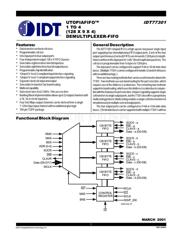
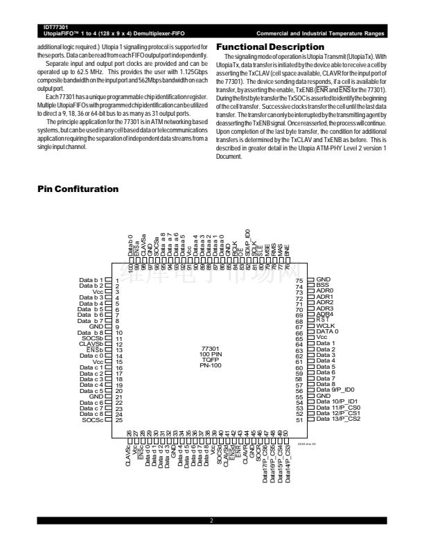
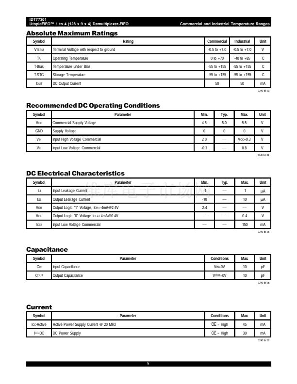
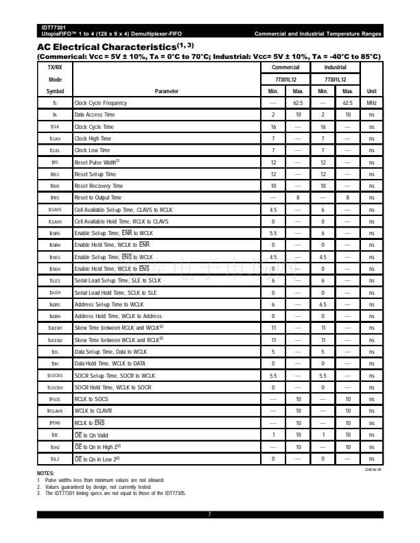
IDT77301
UtopiaFIFO鈩?1 to 4 (128 x 9 x 4) Demultiplexer-FIFO
Commercial and Industrial Temperature Ranges
ENR
is again asserted, the next data byte will be placed in the appropriate
place in memory (no bad data or address will be written).
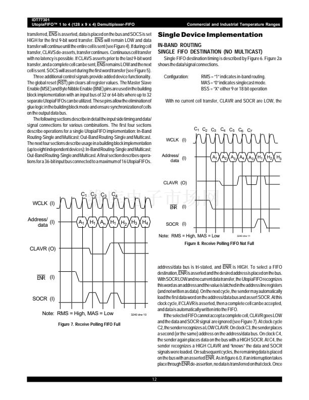
If desired, the sender can wait until a HIGH CLAVR signal before
placing data on the bus; this allows the sender to 鈥減oll鈥?different address鈥檚
on every clock cycle (see figure 8). For cases where an address may not
be available for several cycles, this allows a quicker determination of an
available address. A different address can be polled every clock versus
one every other clock for the prior case. However, there is added latency
once an address is found with an available cell space. Two additional
cycles are needed (C4 and C5) between the address with space available
and actual loading of data (on C6). Once a cell transfer is started (assertion
of SOCR), all data on the address/data bus will be recognized as data, not
as an address. Any assertion of SOCR prior to cell transfer completion
results in an error condition (see cell length error recovery).
Once the current cell transfer is complete, the next cell transfer to the
same FIFO destination can occur with no delay if CLAVR is HIGH before
the next clock cycle鈥檚 rising edge (Clock Cx). No new address is placed
on the bus. A LOW
ENR
combined with a HIGH CLAVR and newly
asserted SOCR indicates the first word of the next cell. The word is written
as data.
If CLAVR is LOW at the end of current cell transfer, the UtopiaFIFO will
interpret the next word as an address. With a LOW CLAVR, an asserted
SOCR on the data on the bus will be ignored.
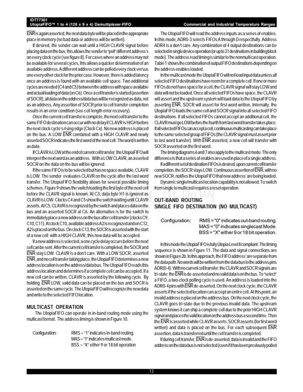
If the same FIFO is to be selected but has no space available, CLAVR
is LOW. The sender evaluates CLAVR on the cycle after the last word
transfer. The UtopiaFIFO flexibility allows for several possible timing
schemes. Figure 9 shows the switch loading the first byte of the next cell
before the CLAVR signal is known. At C3, data byte H1 is ignored as
CLAVR is LOW. Clocks C4 and C5 show the switch waiting until CLAVR
asserts. At C5, CLAVR is recognized by the switch and places data on the
bus and an asserted SOCR at C6. An alternative is for the switch to
immediately place a new address on the bus after cell transfer (clocks C9,
C10, C11). At clock C10, available address A2 is recognized and on C12,
A2 is placed on the bus. On clock C13, the SOCR is asserted with the start
of a new cell; with a HIGH CLAVR, this new data will be accepted.
If a new address is selected, a one cycle delay occurs before the next
cell can be sent. After the current cell transfer is completed, the SOCR and
ENR
stay LOW. CLAVR is a don鈥檛 care. With a LOW SOCR, asserted
ENR,
and no cell transfer taking place, the UtopiaFIFO determines a new
address location is on the address/data bus. The UtopiaFIFO reads this
address location and determines if a complete cell can be accepted. If a
new cell can be written, CLAVR is asserted by the following cycle. By
holding
ENR
LOW, valid data can be placed on the bus and SOCR is
asserted on the same cycle. The UtopiaFIFO will recognize the new data
and write to the selected FIFO location.
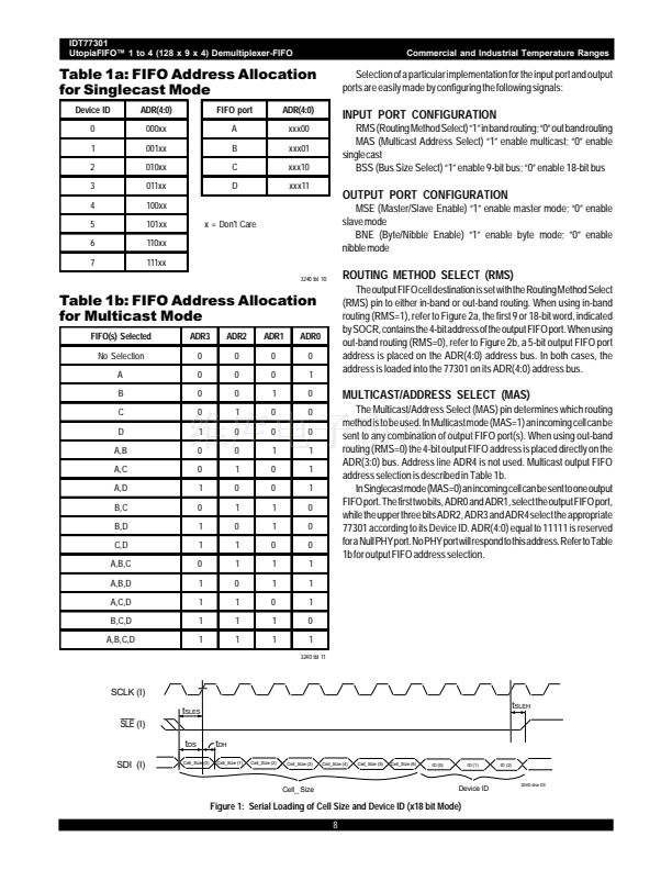
The UtopiaFIFO will read the address inputs as a series of enables.
In this mode, ADR0-3 selects FIFOs A through D respectfully. Address
ADR4 is a don鈥檛 care. Any combination of 4 output destinations can be
selected in single device operation (or up to 31 destinations in building block
mode). The address read timing is similar to the nonmulticast operation.
Table 1 shows the combination of output FIFO destinations depending on
the address enables loaded.
In the multicast mode the UtopiaFIFO will not load input data unless all
selected FIFO destinations have room for a complete cell. If one or more
FIFOs do not have space for a cell, the CLAVR signal will stay LOW and
data will not be loaded. Once all selected FIFOs have space, the CLAVR
will assert and the upstream system will load data to the UtopiaFIFO by
asserting
ENR.
SOCR will assert for first word written. Internally, the
UtopiaFIFO loads the same cell and SOCR signal into all selected FIFO
destinations. If all selected FIFOs cannot accept an additional cell, the
CLAVR must go LOW before the fourth from last word transfer takes place.
If all selected FIFOs can accept a cell, continuous multicasting can take place
to the same selected group of FIFOs (the CLAVR signal must assert prior
to last word transfer). With
ENR
asserted, a new cell will transfer with
SOCR asserted on the first word.
The timing diagrams 6 and 7 also apply to the multicast mode. The only
difference is that a series of enables are used in place of a single address.
If a different set of destination FIFOs is desired, upon current cell transfer
completion, the SOCR stays LOW. Continuous assertion of
ENR,
with no
new SOCR, notifies the UtopiaFIFO that new address鈥?are being loaded.
Dynamic single/multicast location capability is not allowed. To switch
from single to multicast requires a reset operation.
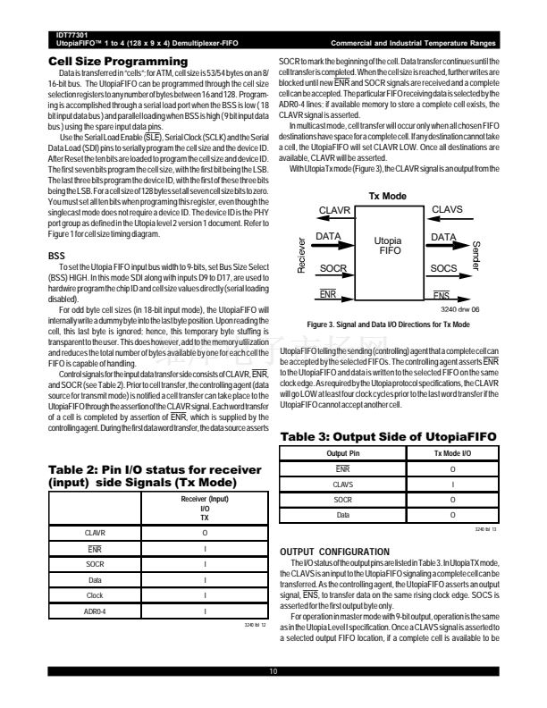
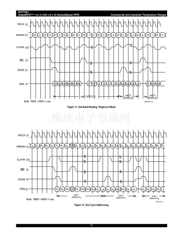
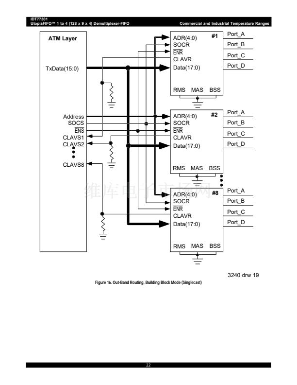
OUT-BAND ROUTING
SINGLE FIFO DESTINATION (NO MULTICAST)
Configuration:
RMS = "0" indicates out-band routing.
MAS = "0" indicates singlecast Mode.
BSS = "X" either 9 or 18 bit operation.
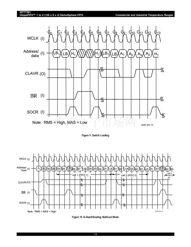
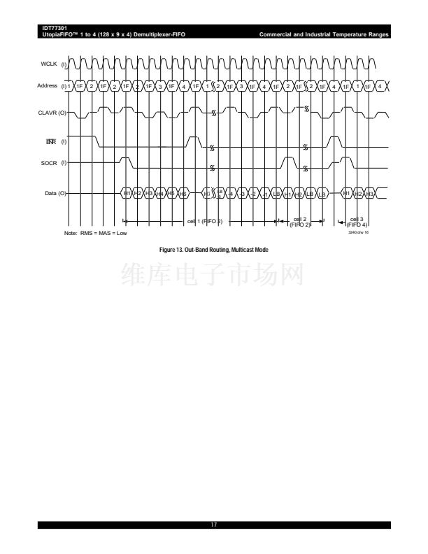
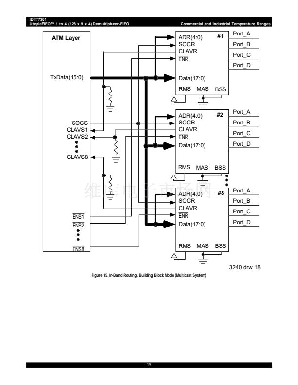
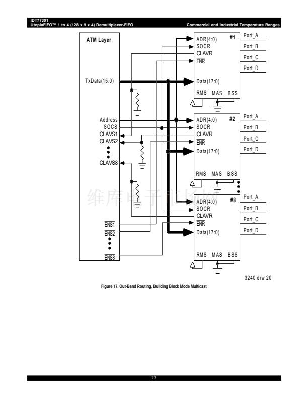
MULTICAST OPERATION
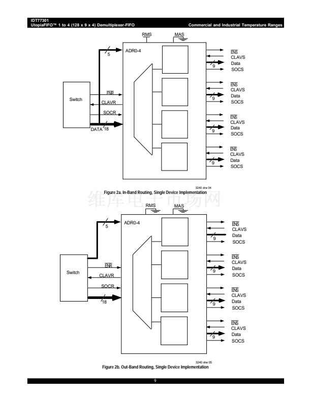
The UtopiaFIFO can operate in in-band routing mode using the
multicast format. The address timing is shown in Figure 10.
Configuration:
RMS = 鈥?鈥?indicates in-band routing.
MAS = 鈥?鈥?indicates multicast mode.
BSS = 鈥淴鈥?either 9 or 18 bit operation
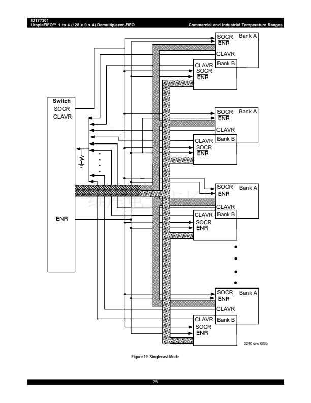
In this mode the UtopiaFIFO is fully Utopia Level II compliant. The timing
sequence is shown in Figure 11. The data and signal connections are
shown in Figure 2b. In this approach, the FIFO address鈥?are separate from
the data path. No words will be written from the data bus to the address pins
ADR(0-4). With no current cell transfer: the CLAVR and SOCR signals are
tri-state; the
ENR
is de-asserted and no valid data is on the bus. To 鈥渟elect鈥?/div>
a FIFO, a two-clock polling cycle is used. An address is loaded into the
ADR0-4 pins with
ENR
de-asserted. On the next clock cycle, the CLAVR
asserts if the selected location can accept an entire cell. At this point, an
invalid address is placed on the address bus. On the next clock cycle, the
CLAVR goes tri-state due to the previous invalid data. The upstream
system knows it can ship a complete cell due to the prior HIGH CLAVR
signal and places the valid location on the address bus a second time. Then
the
ENR
is asserted while CLAVR asserts. SOCR asserts (for first word
written) and data is placed on the bus. For each subsequent
ENR
assertion, data is transferred until the cell transfer is completed.
If during cell transfer,
ENR
is de-asserted, data is invalid and the FIFO
address on the data bus is not selected (even if it has been previously polled
13


 1
1
 2
2
 3
3
 4
4
 5
5
 6
6
 7
7
 8
8
 9
9
 10
10
 11
11
 12
12
 13
13
 14
14
 15
15
 16
16
 17
17
 18
18
 19
19
 20
20
 21
21
 22
22
 23
23
 24
24
 25
25
 26
26
 27
27
 28
28
 29
29
