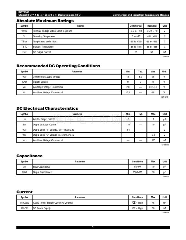
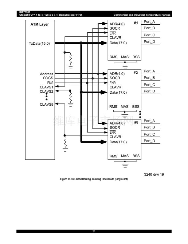
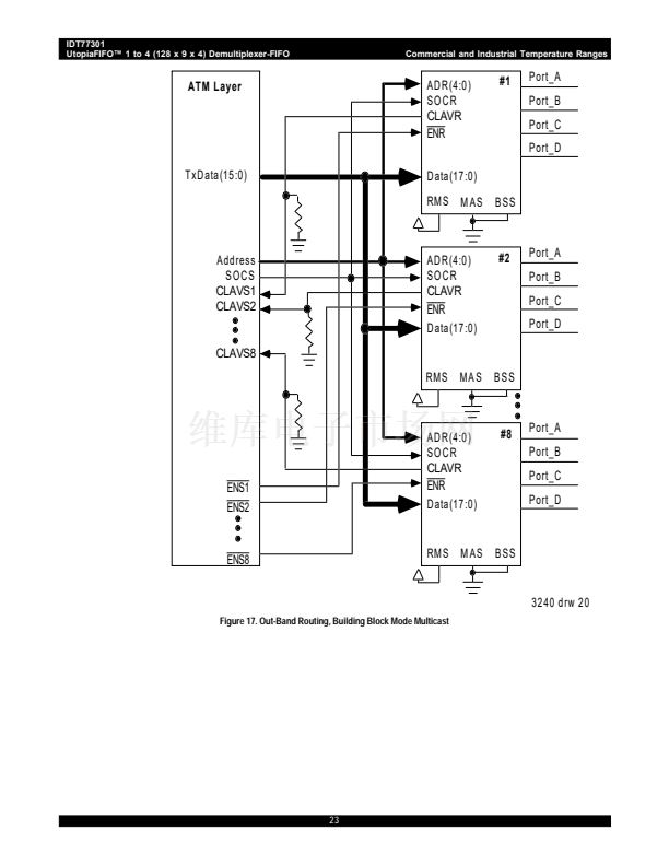
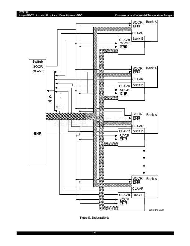
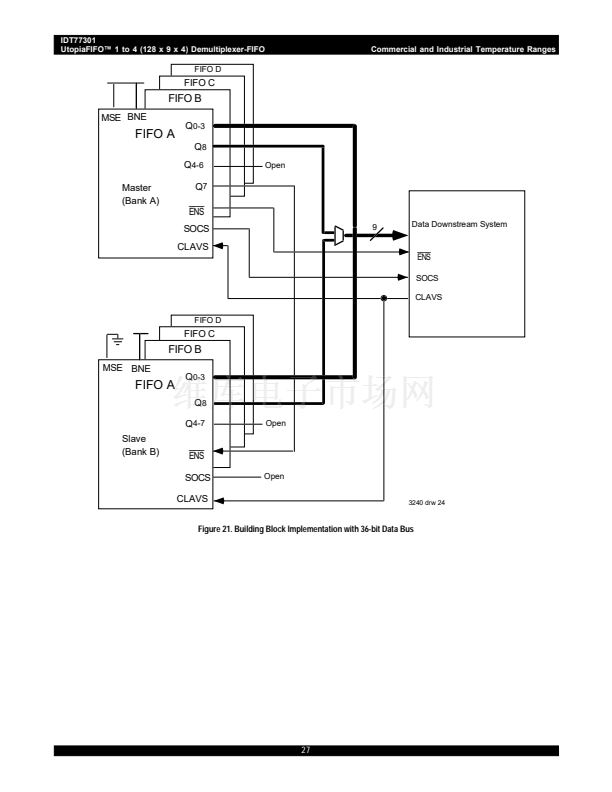
IDT77301
UtopiaFIFO鈩?1 to 4 (128 x 9 x 4) Demultiplexer-FIFO
Commercial and Industrial Temperature Ranges
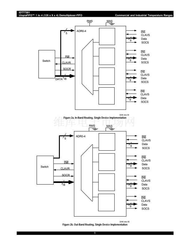
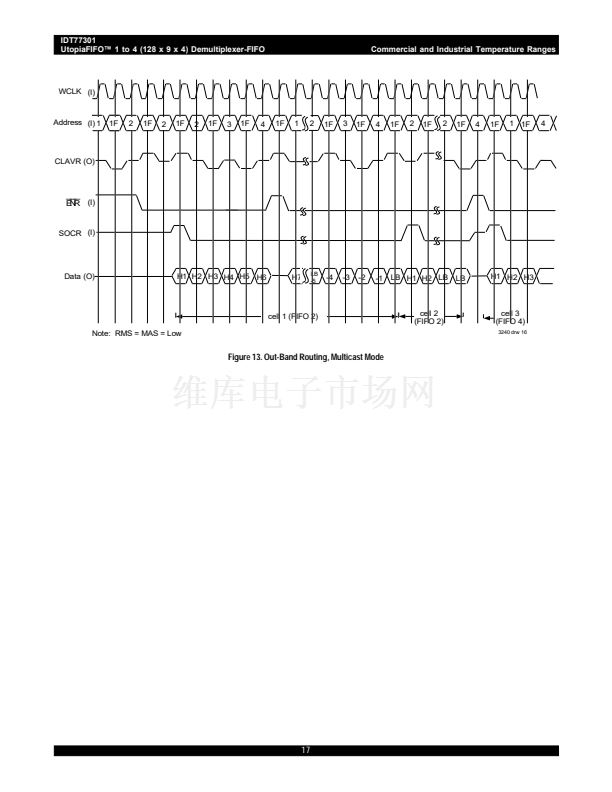
additional logic required.) Utopia 1 signalling protocol is supported for
these ports. Data can be read from each FIFO output port independently.
Separate input and output port clocks are provided and can be
operated up to 62.5 MHz. This provides the user with 1.125Gbps
composite bandwidth on the input port and 562Mbps bandwidth on each
output port.
Each 77301 has a unique programmable chip identification register.
Multiple UtopiaFIFOs with programmed chip identification can be utilized
to direct a 9, 18, 36 or 64-bit bus to as many as 31 output ports.
The principle application for the 77301 is in ATM networking based
systems, but can be used in any cell based data or telecommunications
application requiring the separation of independent data streams from a
single input channel.
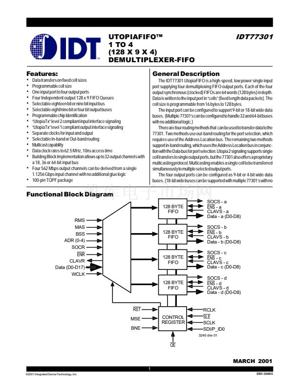
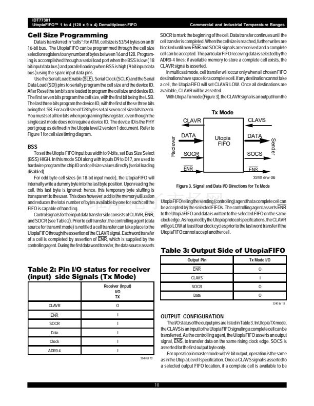
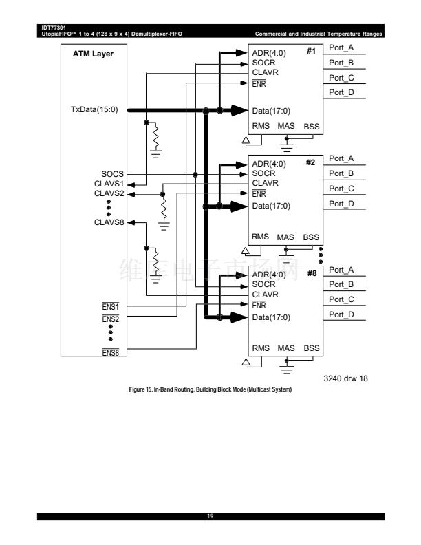
.unctional Description
The signaling mode of operation is Utopia Transmit (UtopiaTx). With
UtopiaTx, data transfer is initiated by the device able to receive a cell by
asserting the TxCLAV (cell space available, CLAVR for the input port of
the 77301). The device sending data responds, if a cell is available for
transfer, by asserting the enable, TxENB (ENR and
ENS
for the 77301).
During the first byte transfer the TxSOC is asserted to identify the beginning
of the cell transfer. Successive clocks transfer the cell until the last data
transfer. The transfer can only be interrupted by the transmitting agent by
deasserting the TxENB signal. Once reasserted, the process will continue.
Upon completion of the last byte transfer, the condition for additional
transfers is determined by the TxCLAV and TxENB as before. This is
described in greater detail in the Utopia ATM-PHY Level 2 version 1
Document.
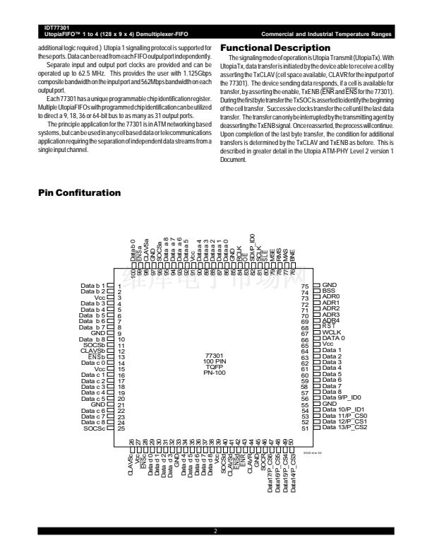
Pin Confituration
ENS
a
CLAVSa
GND
SOCSa
Data a 8
Data a 7
Data a 6
Data a 5
Vcc
Data a 4
Data a 3
Data a 2
Data a 1
Data a 0
GND
RCLK
SDI/P_ID0
SCLK
Data b 0
100
99
98
97
96
95
94
93
92
91
90
89
88
87
86
85
84
83
82
81
80
79
78
77
76
SLE
OE
MSE
RMS
MAS
BNE
Data b 1
Data b 2
Vcc
Data b 3
Data b 4
Data b 5
Data b 6
Data b 7
GND
Data b 8
SOCSb
CLAVSb
ENS
b
Data c 0
Vcc
Data c 1
Data c 2
Data c 3
Data c 4
Data c 5
GND
Data c 6
Data c 7
Data c 8
SOCSc
1
2
3
4
5
6
7
8
9
10
11
12
13
14
15
16
17
18
19
20
21
22
23
24
25
77301
100 PIN
TQFP
PN-100
75
74
73
72
71
70
69
68
67
66
65
64
63
62
61
60
59
58
57
56
55
54
53
52
51
GND
BSS
ADR0
ADR1
ADR2
ADR3
ADR4
WCLK
DATA 0
Vcc
Data 1
Data 2
Data 3
Data 4
Data 5
Data 6
Data 7
Data 8
Data 9/P_ID0
GND
Data 10/P_ID1
Data 11/P_CS0
Data 12/P_CS1
Data 13/P_CS2
RST
26
27
28
29
30
31
32
33
34
35
36
37
38
39
40
41
42
43
44
45
46
47
48
49
50
2
CLAVR
GND
SOCR
Data17/P_CS6
Data16/P_CS5
Data15/P_CS4
Data14/P_CS3
CLAVSc
Vcc
ENS
c
Data d 0
Data d 1
Data d 2
Data d 3
GND
Data d 4
Data d 5
Data d 6
Data d 7
Data d 8
Vcc
SOCSd
CLAVSd
ENS
d
ENR
3 2 4 0 d rw 0 2


 1
1
 2
2
 3
3
 4
4
 5
5
 6
6
 7
7
 8
8
 9
9
 10
10
 11
11
 12
12
 13
13
 14
14
 15
15
 16
16
 17
17
 18
18
 19
19
 20
20
 21
21
 22
22
 23
23
 24
24
 25
25
 26
26
 27
27
 28
28
 29
29
