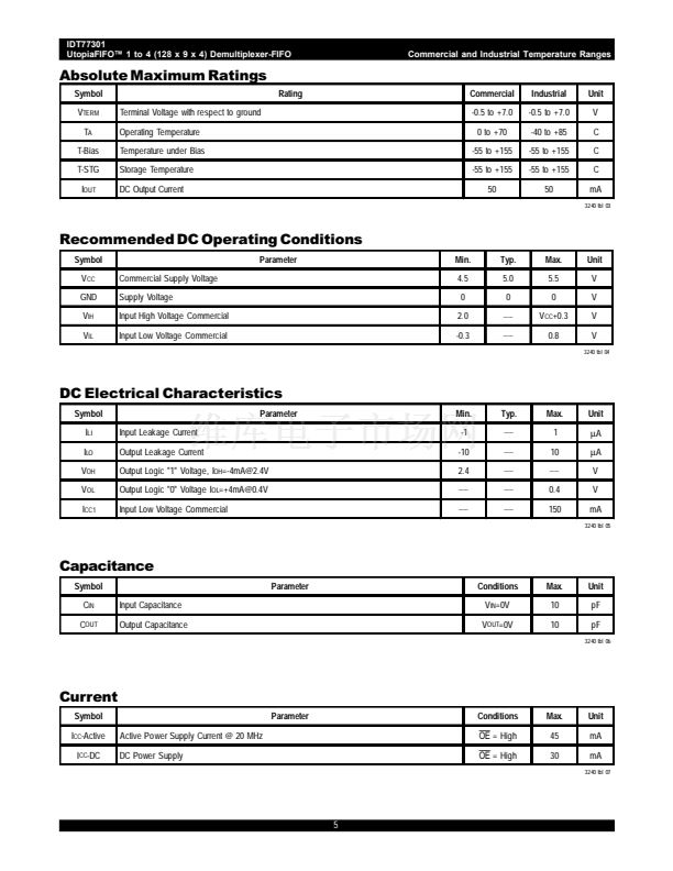
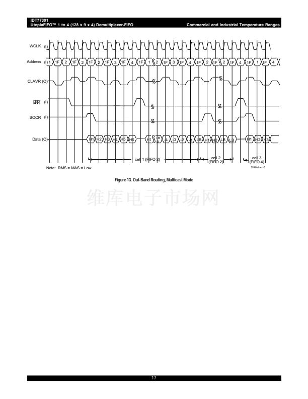
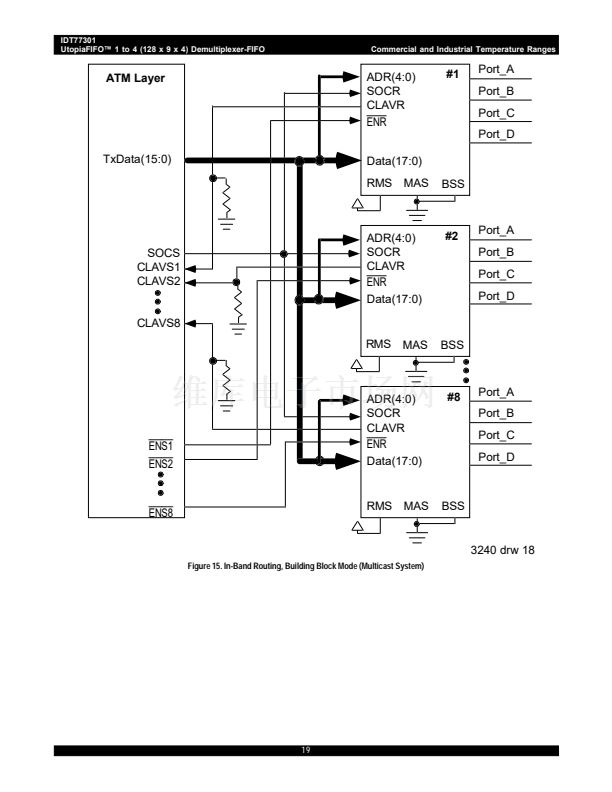
IDT77301
UtopiaFIFO鈩?1 to 4 (128 x 9 x 4) Demultiplexer-FIFO
Commercial and Industrial Temperature Ranges
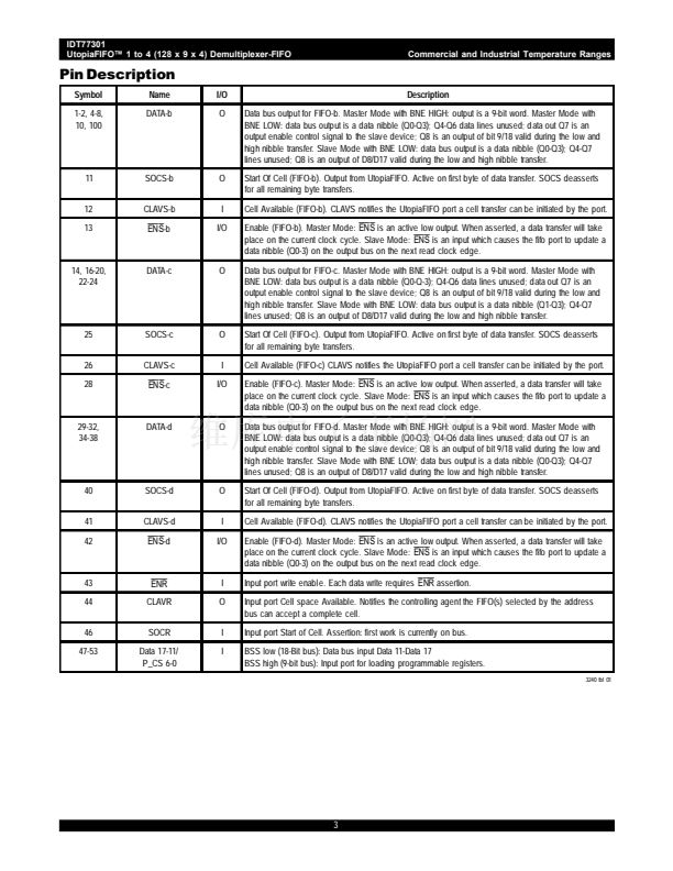
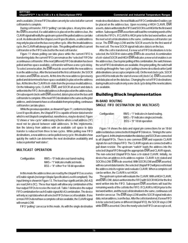
Pin Description
Symbol
54, 56
57-64, 66
68
69-73
Name
Data 9-10 /
P_ID 0-1
Data 0-8
I/O
I
I
I
I
Description
18-Bit bus: Data bus input
9-bit bus: Parallel programmable register load (ID0, ID1)
Data bus input
Reset. Clears all FIFO memory locations, cell size read/write pointers.
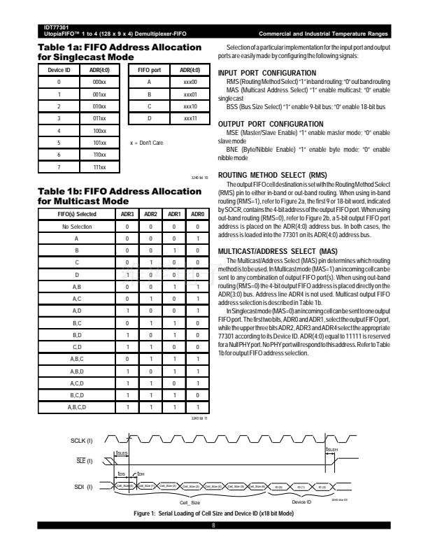
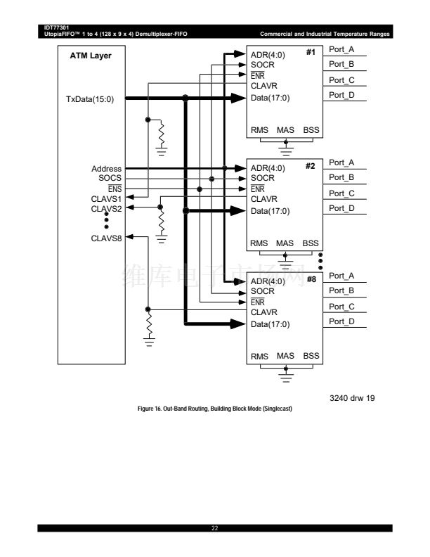
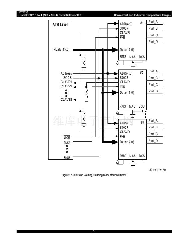
Address Location(s). Provide cell destination and multicast addresses. Singlecast Operation: for out-
band routing, address location is loaded from incoming Utopia Level 2 compliant address lines; for
in-band routing, address location is derived from data lines D0-D17 (see Table 1a). Multicast
Operation for out-band routing, the ADR0-3 signals (ADR4 is not used) act as enables which select
the desired output FIFO combination (see Table 1b); for in-band routing, the output FIFO
co mbindation is derived from the data lines D0-D17.
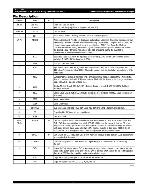
Bus Size Select. BSS HIGH, the input bus is set to 9-bits (D0-D8) and D9-D17 determine cell size
and chip ID. BSS LOW, the input bus is 18-bits.
Input port Data write clock.
Byte Nibble Enable. BNE HIGH, output ports are byte wide data buses. BNE LOW, output data is in
4-bit "nibble" increments using Q0-Q3. This mode supports wide input data bus applications of 32 to
72-bit widths.
Multicast/Address Select. Determines single or multicast input mode. Selecting MAS HIGH sets the
device to multicast mode with ADR0-3 as enables. MAS LOW the device is set to single destination
mode with ADR0-4 lines as address lines.
Routing Method Select. With RMS HIGH, In-band Routing is selected. With RMS LOW, Out-band
Routing is selected.
Master Slave Enable. With MSE set HIGH, device is set as a master; with MSE LOW, device is set
as a slave.
Serial Load Enable.
Serial Load Clock.
BSS low, Serial data load. BSS high Serial input port for loading programmable registers.
Output Enable. Tri-States all data output buses.
Data read clock.
Data bus output for FIFO-a. Master Mode with BNE HIGH: output is a 9-bit word. Master Mode with
BNE LOW: data bus output is a data nibble (Q0-Q3); Q4-Q6 data lines unused; data out Q7 is an
output enable control signal to the slave device; Q8 is an output of bit 9/18 valid during the low and
high nibble transfer. Slave Mode with BNE LOW: data bus output is a data nibble (Q0-Q3); Q4-Q7
lines unused; Q8 is an output of D8/D17 valid during the low and high nibble transfer.
Start Of Cell (FIFO-a) output from UtopiaFIFO. Active on first byte of data transfer. SOCS deasserts for
all remaining byte transfers.
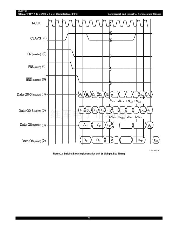
Cell Available (FIFO-a). CLAVS notifies the UtopiaFIFO port. A cell transfer can be initiated by
the port.
Enable (FIFO-a). Master Mode:
ENS
is an active low output. When asserted, a data transfer will take
place on the current clock cycle. Slave Mode:
ENS
is an input which causes the fifo port to update a
data nibble (Q0-3) on the output bus on the next read clock edge.
Lo gic and supply ground pins 9, 21, 33, 45, 55, 75, 85 and 97.
Logic and supply V
CC
pins 3, 15, 27, 39, 65, and 91.
3240 tbl 02
RST
ADR0-4
74
67
76
BSS
WCLK
BNE
I
I
I
77
MAS
I
78
79
80
81
82
83
84
86-90,
92-95
RMS
MSE
I
I
I
I
I
I
I
O
SLE
SCLK
SDI/P_ID0
OE
RCLK
DATA-a
96
98
99
SOCS-1
CLAVS-a
O
I
I/O
ENS
-s
GND
V
CC
____
____
4


 1
1
 2
2
 3
3
 4
4
 5
5
 6
6
 7
7
 8
8
 9
9
 10
10
 11
11
 12
12
 13
13
 14
14
 15
15
 16
16
 17
17
 18
18
 19
19
 20
20
 21
21
 22
22
 23
23
 24
24
 25
25
 26
26
 27
27
 28
28
 29
29
