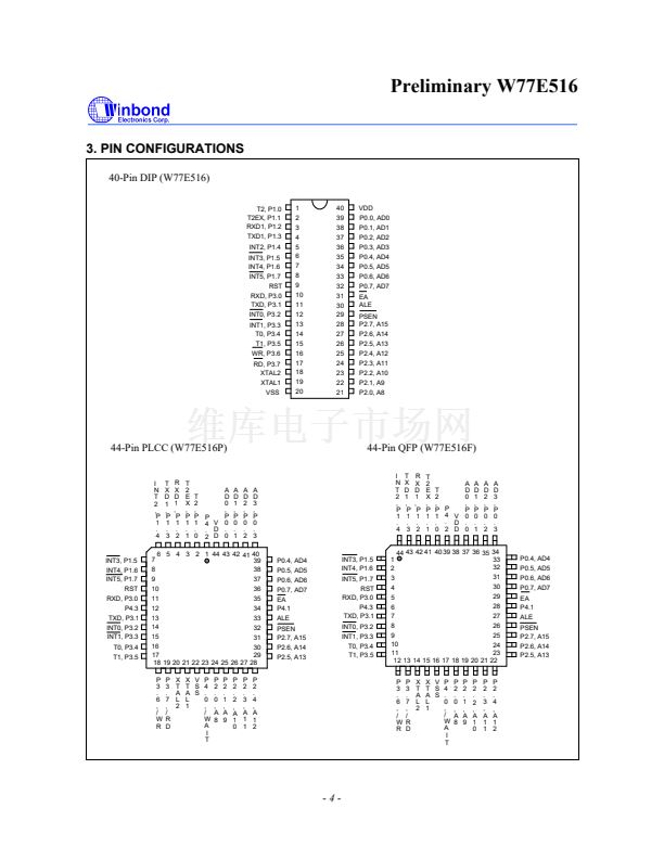
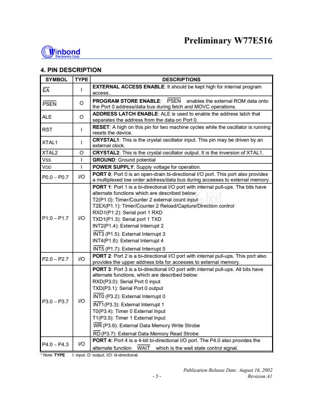
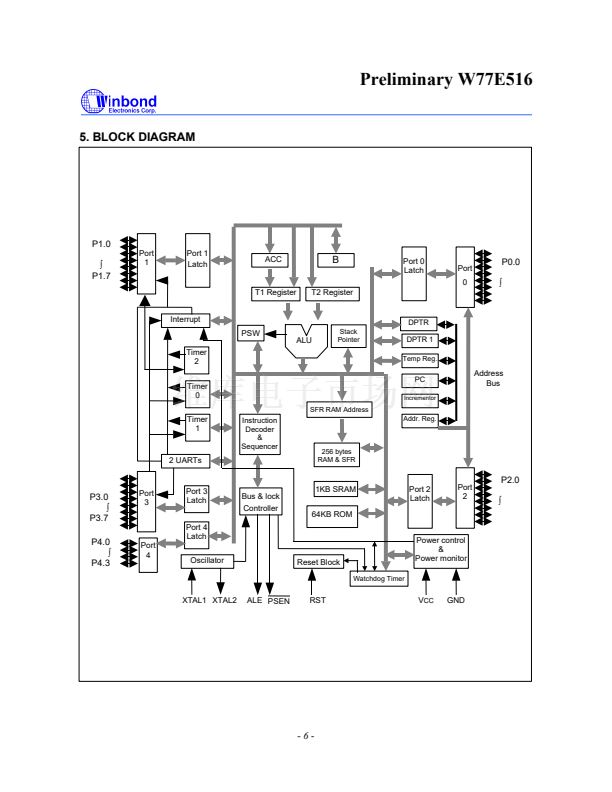
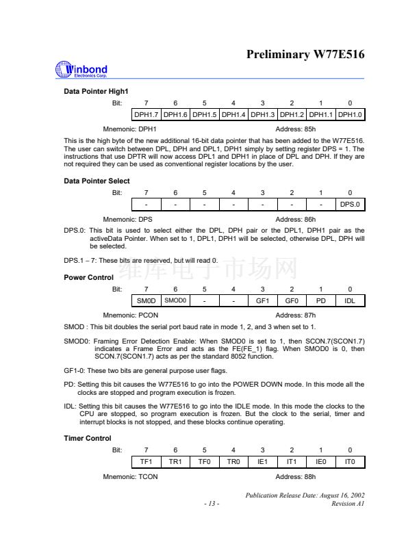
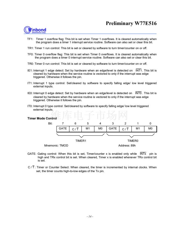
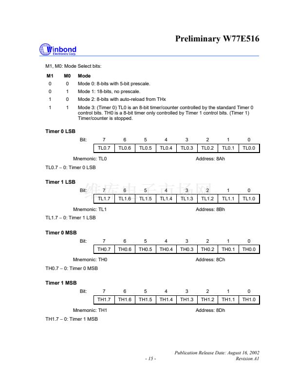
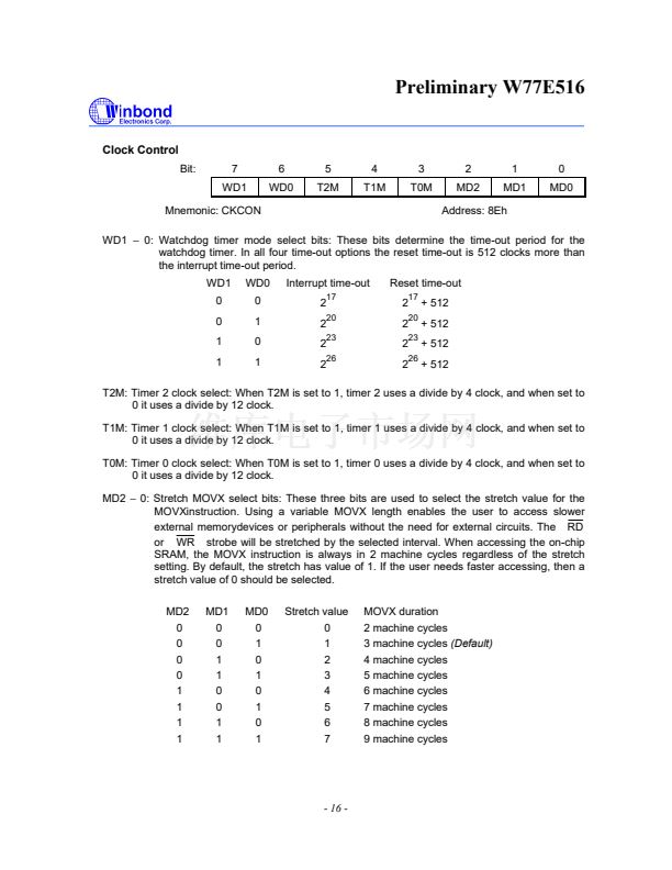
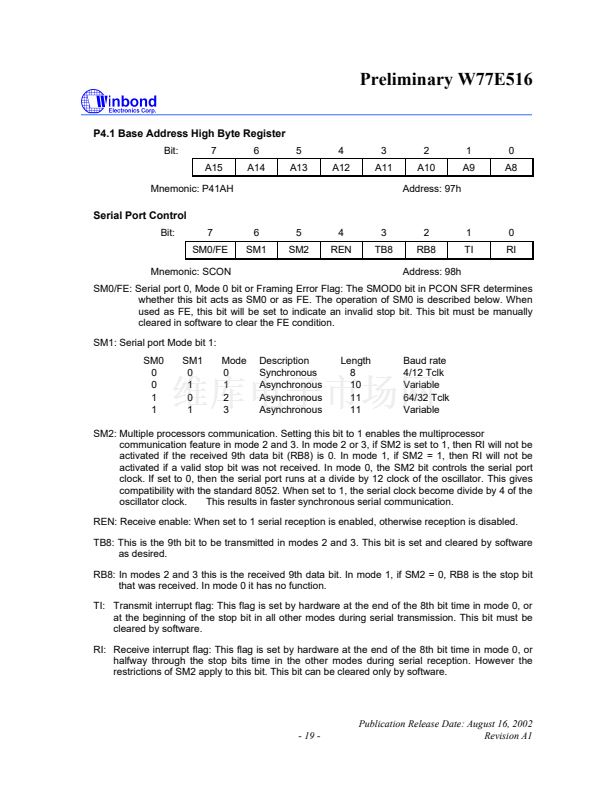
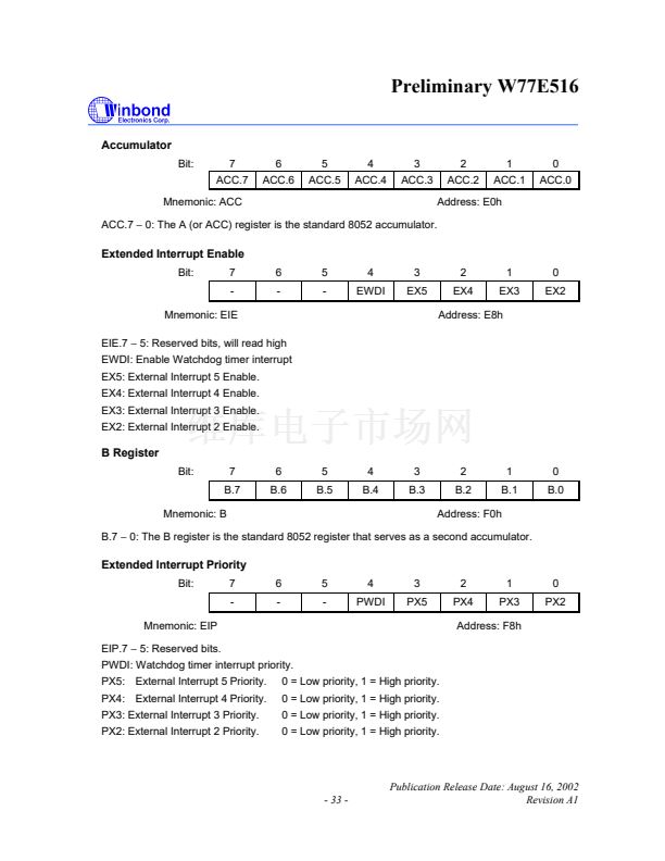
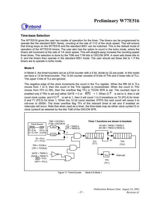
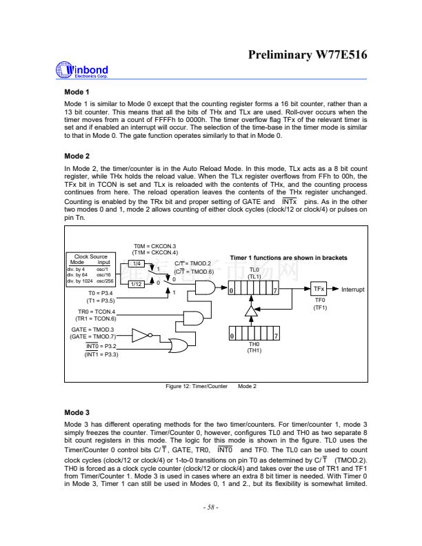
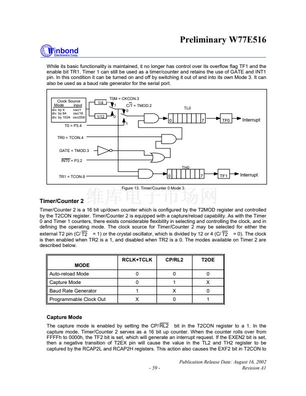
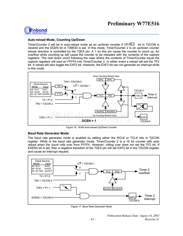
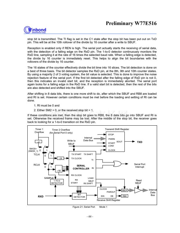
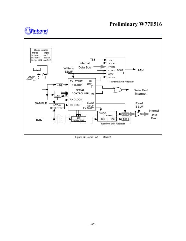
鈭?/div>
0: Serial data on the serial port 0 is read from or written to this location. It actually
consists of two separate internal 8-bit registers. One is the receive resister, and the
other is the transmit buffer. Any read access gets data from the receive data buffer,
while write access is to the transmit data buffer.
P4.2 Base Address Low Byte Register
Bit:
7
A7
Mnemonic: P42AL
6
A6
5
A5
4
A4
3
A3
2
A2
Address: 9Ah
1
A1
0
A0
P4.2 Base Address High Byte Register
Bit:
7
A15
Mnemonic: P42AH
6
A14
5
A13
4
A12
3
A11
2
A10
Address: 9Bh
1
A9
0
A8
P4.3 Base Address Low Byte Register
Bit:
7
A7
Mnemonic: P43AL
6
A6
5
A5
4
A4
3
A3
2
A2
Address: 9Ch
1
A1
0
A0
P4.3 Base Address High Byte Register
Bit:
7
A15
Mnemonic: P43AH
6
A14
5
A13
4
A12
3
A11
2
A10
Address: 9Dh
1
A9
0
A8
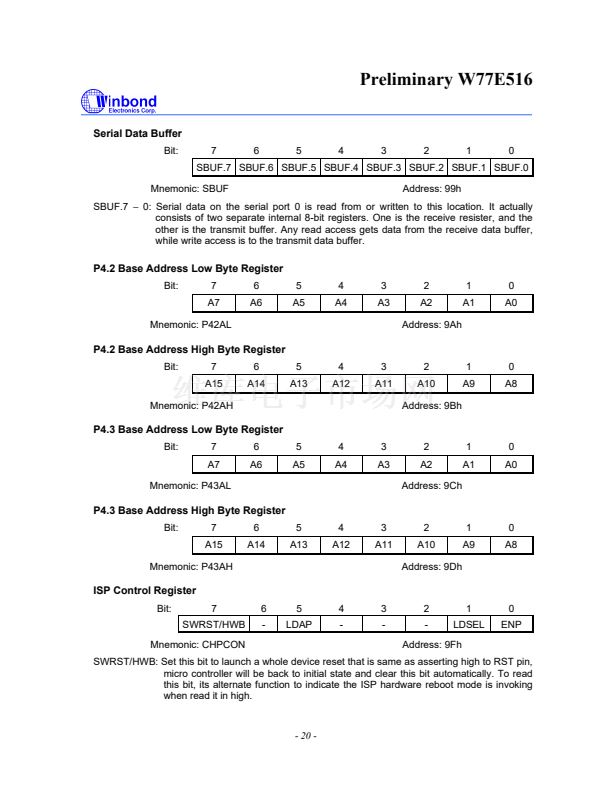
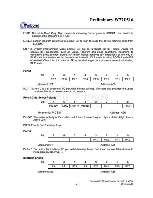
ISP Control Register
Bit:
7
SWRST/HWB
Mnemonic: CHPCON
6
-
5
LDAP
4
-
3
-
2
-
1
LDSEL
0
ENP
Address: 9Fh
SWRST/HWB: Set this bit to launch a whole device reset that is same as asserting high to RST pin,
micro controller will be back to initial state and clear this bit automatically. To read
this bit, its alternate function to indicate the ISP hardware reboot mode is invoking
when read it in high.
- 20 -


 1
1
 2
2
 3
3
 4
4
 5
5
 6
6
 7
7
 8
8
 9
9
 10
10
 11
11
 12
12
 13
13
 14
14
 15
15
 16
16
 17
17
 18
18
 19
19
 20
20
 21
21
 22
22
 23
23
 24
24
 25
25
 26
26
 27
27
 28
28
 29
29
 30
30
 31
31
 32
32
 33
33
 34
34
 35
35
 36
36
 37
37
 38
38
 39
39
 40
40
 41
41
 42
42
 43
43
 44
44
 45
45
 46
46
 47
47
 48
48
 49
49
 50
50
 51
51
 52
52
 53
53
 54
54
 55
55
 56
56
 57
57
 58
58
 59
59
 60
60
 61
61
 62
62
 63
63
 64
64
 65
65
 66
66
 67
67
 68
68
 69
69
 70
70
 71
71
 72
72
 73
73
 74
74
 75
75
 76
76
 77
77
 78
78
 79
79
 80
80
 81
81
 82
82
 83
83
 84
84
 85
85
