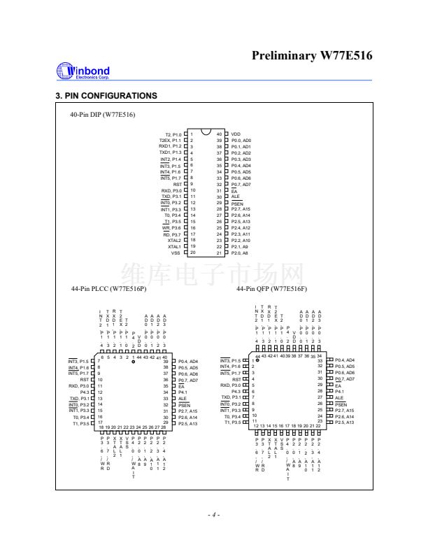
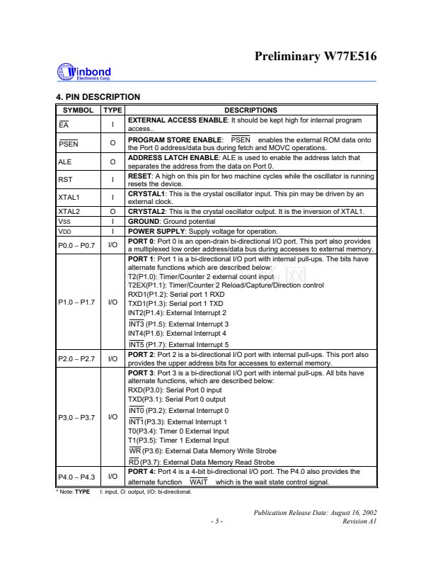
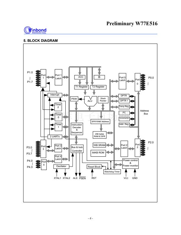
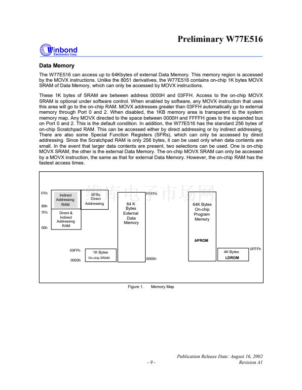
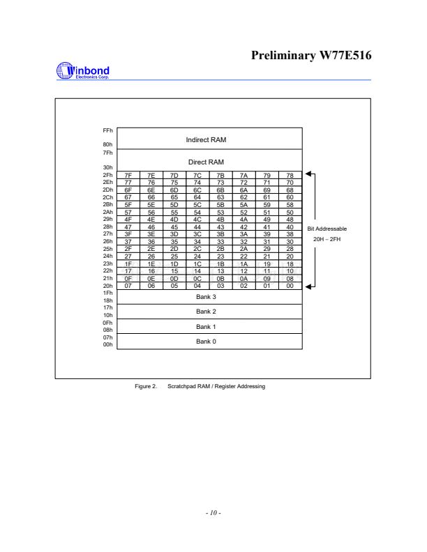
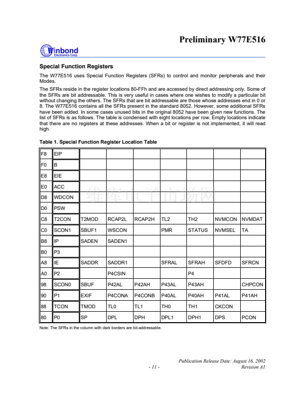
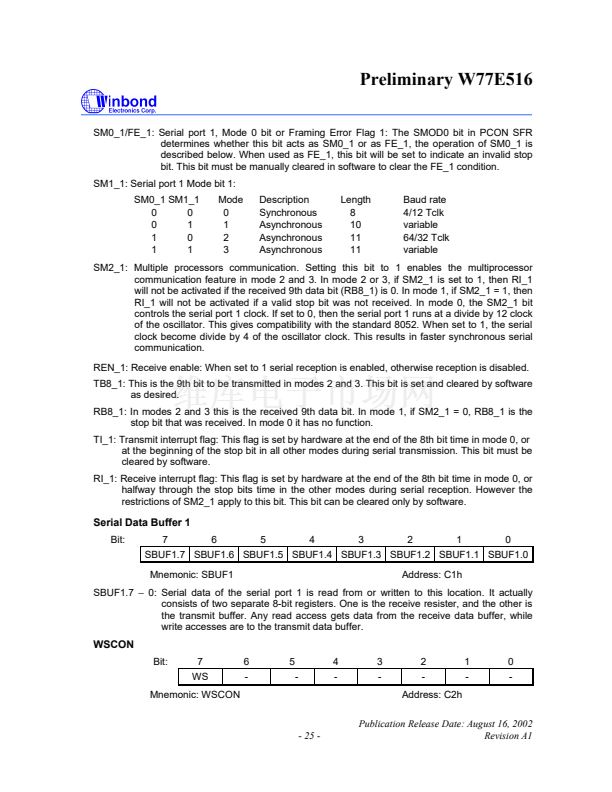
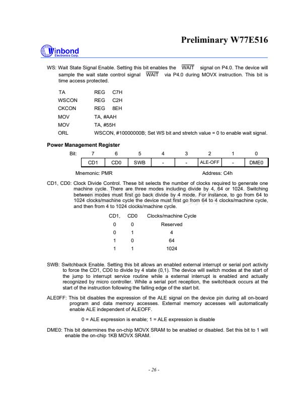
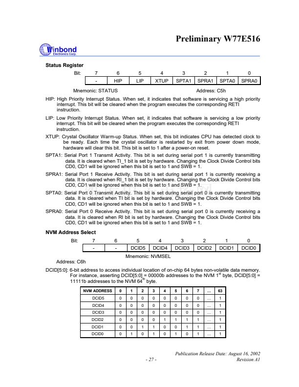
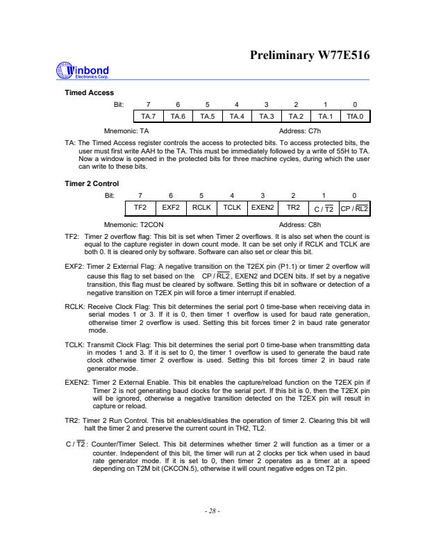
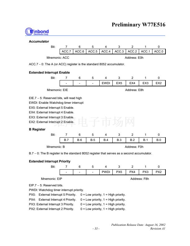
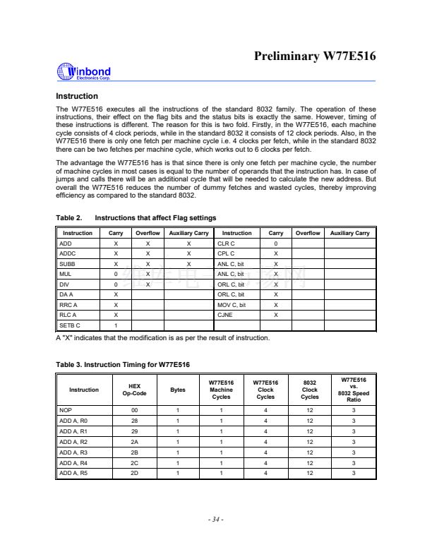
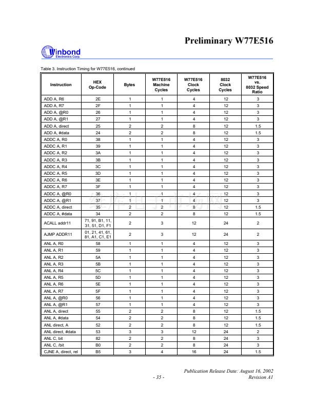
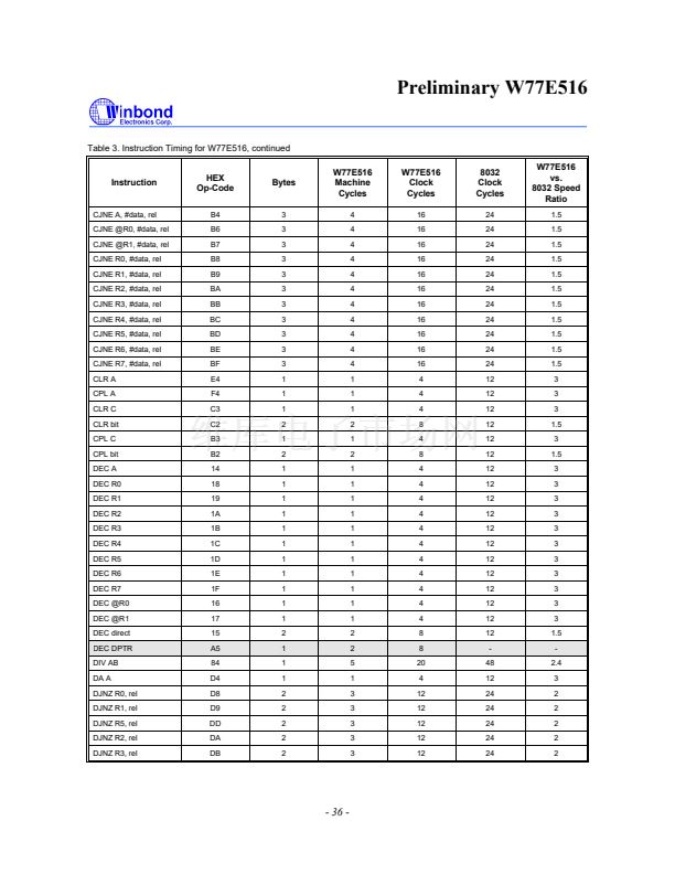
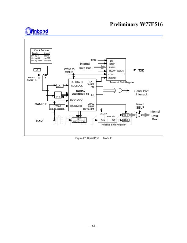
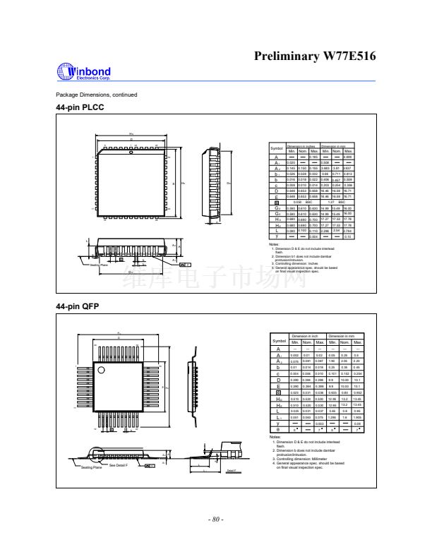
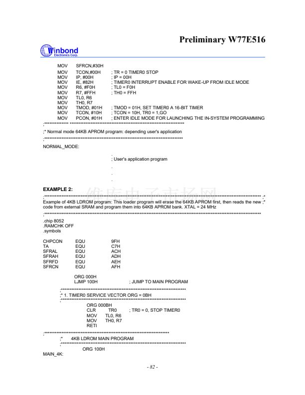
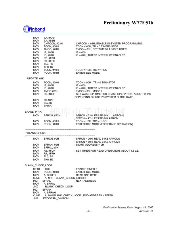
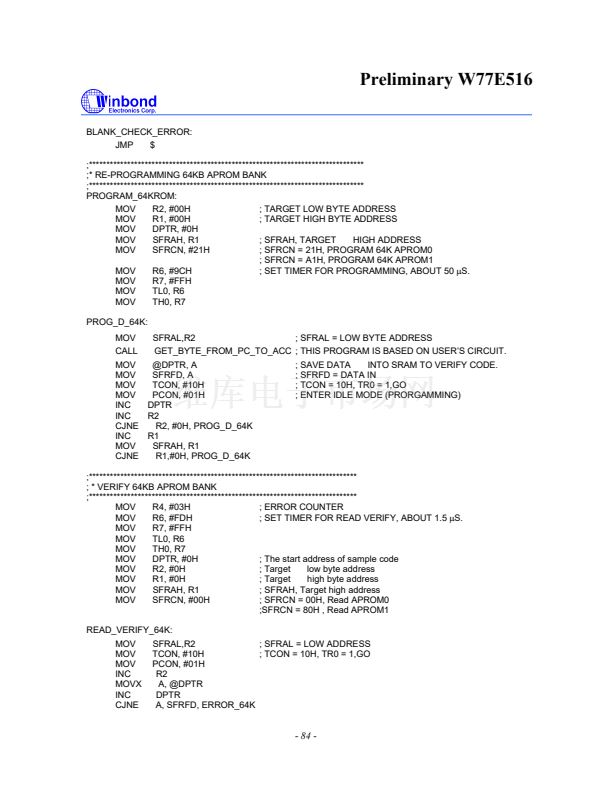
Preliminary W77E516
instruction being executed, then an additional delay is introduced. The maximum response time (if
no other interrupt is in service) occurs if the W77E516 is performing a write to IE, IP, EIE or EIP and
then executes a MUL or DIV instruction. From the time an interrupt source is activated, the longest
reaction time is 12 machine cycles. This includes 1 machine cycle to detect the interrupt, 2 machine
cycles to complete the IE, IP, EIE or EIP access, 5 machine cycles to complete the MUL or DIV
instruction and 4 machine cycles to complete the hardware LCALL to the interrupt vector location.
Thus in a single-interrupt system the interrupt response time will always be more than 5 machine
cycles and not more than 12 machine cycles. The maximum latency of 12 machine cycle is 48 clock
cycles. Note that in the standard 8051 the maximum latency is 8 machine cycles which equals 96
machine cycles. This is a 50% reduction in terms of clock periods.
8. PROGRAMMABLE TIMERS/COUNTERS
The W77E516 has three 16-bit programmable timer/counters and one programmable Watchdog timer.
The Watchdog timer is operationally quite different from the other two timers.
Timer/Counters 0 & 1
The W77E516 has two 16-bit Timer/Counters. Each of these Timer/Counters has two 8 bit registers
which form the 16 bit counting register. For Timer/Counter 0 they are TH0, the upper 8 bits register,
and TL0, the lower 8 bit register. Similarly Timer/Counter 1 has two 8 bit registers, TH1 and TL1. The
two can be configured to operate either as timers, counting machine cycles or as counters counting
external inputs.
When configured as a "Timer", the timer counts clock cycles. The timer clock can be programmed to
be thought of as 1/12 of the system clock or 1/4 of the system clock. In the "Counter" mode, the
register is incremented on the falling edge of the external input pin, T0 in case of Timer 0, and T1 for
Timer 1. The T0 and T1 inputs are sampled in every machine cycle at C4. If the sampled value is high
in one machine cycle and low in the next, then a valid high to low transition on the pin is recognized
and the count register is incremented. Since it takes two machine cycles to recognize a negative
transition on the pin, the maximum rate at which counting will take place is 1/24 of the master clock
frequency. In either the "Timer" or "Counter" mode, the count register will be updated at C3. Therefore,
in the "Timer" mode, the recognized negative transition on pin T0 and T1 can cause the count register
value to be updated only in the machine cycle following the one in which the negative edge was
detected.
The "Timer" or "Counter" function is selected by the "C/ T " bit in the TMOD Special Function Register.
Each Timer/Counter has one selection bit for its own; bit 2 of TMOD selects the function for
Timer/Counter 0 and bit 6 of TMOD selects the function for Timer/Counter 1. In addition each
Timer/Counter can be set to operate in any one of four possible modes. The mode selection is done by
bits M0 and M1 in the TMOD SFR.
- 56 -


 1
1
 2
2
 3
3
 4
4
 5
5
 6
6
 7
7
 8
8
 9
9
 10
10
 11
11
 12
12
 13
13
 14
14
 15
15
 16
16
 17
17
 18
18
 19
19
 20
20
 21
21
 22
22
 23
23
 24
24
 25
25
 26
26
 27
27
 28
28
 29
29
 30
30
 31
31
 32
32
 33
33
 34
34
 35
35
 36
36
 37
37
 38
38
 39
39
 40
40
 41
41
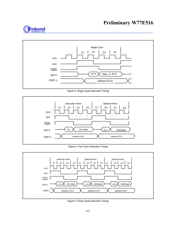 42
42
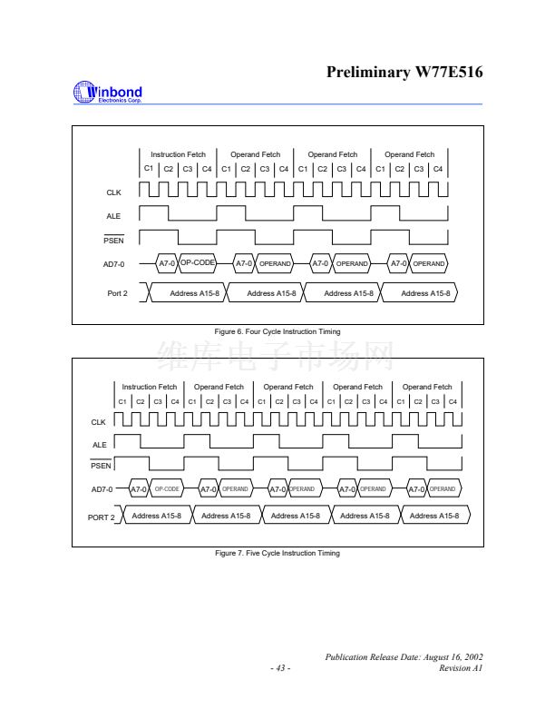 43
43
 44
44
 45
45
 46
46
 47
47
 48
48
 49
49
 50
50
 51
51
 52
52
 53
53
 54
54
 55
55
 56
56
 57
57
 58
58
 59
59
 60
60
 61
61
 62
62
 63
63
 64
64
 65
65
 66
66
 67
67
 68
68
 69
69
 70
70
 71
71
 72
72
 73
73
 74
74
 75
75
 76
76
 77
77
 78
78
 79
79
 80
80
 81
81
 82
82
 83
83
 84
84
 85
85
