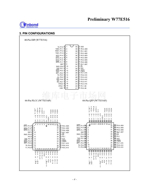
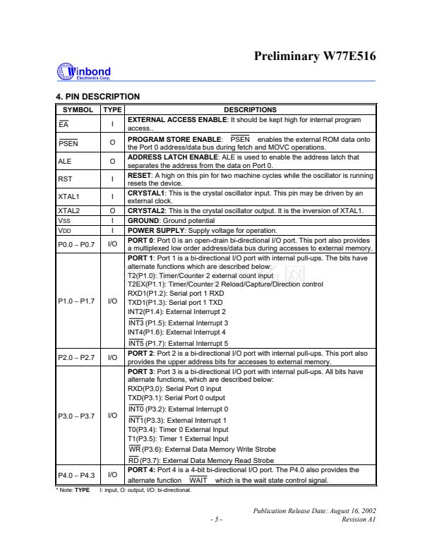
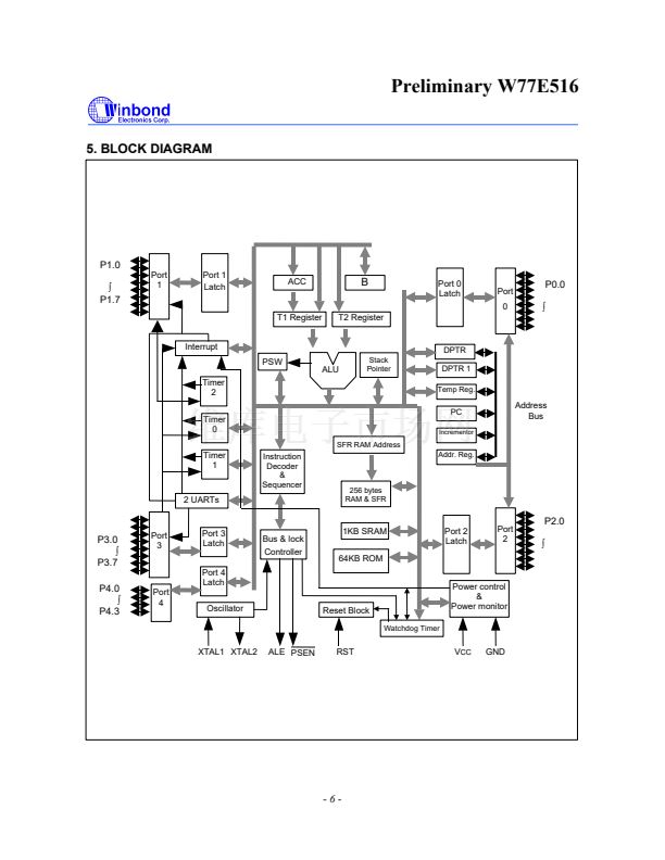
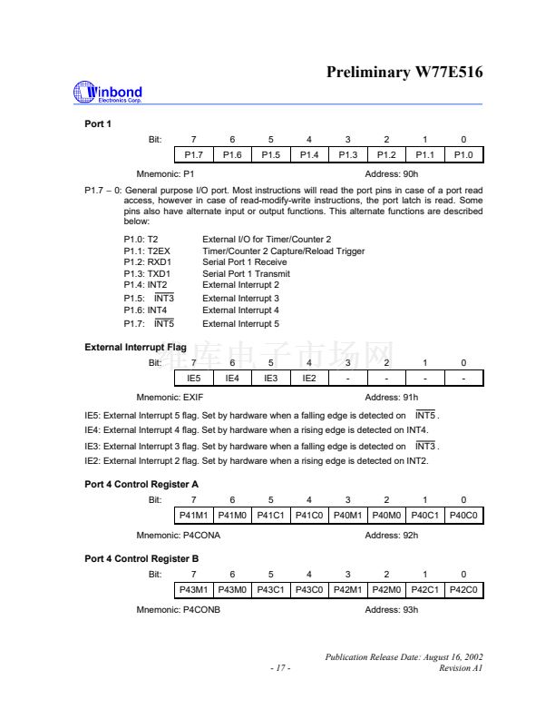
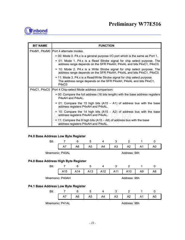
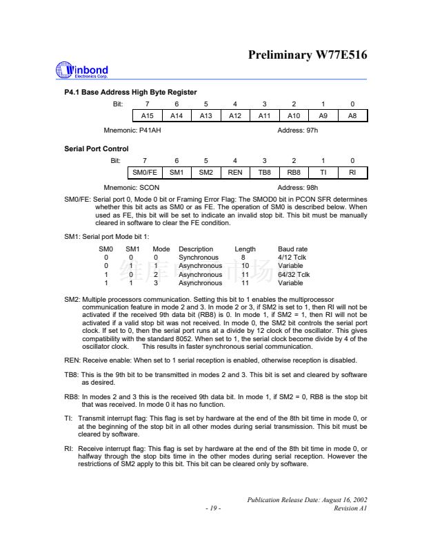
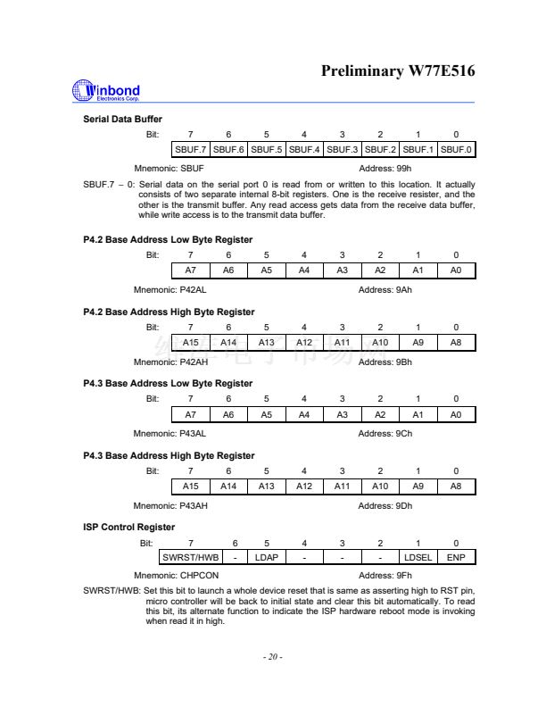
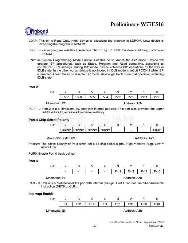
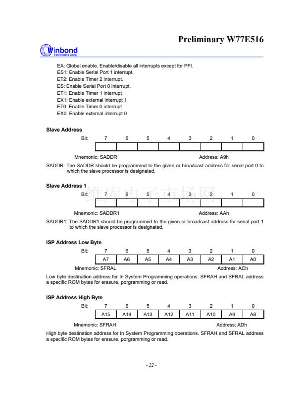
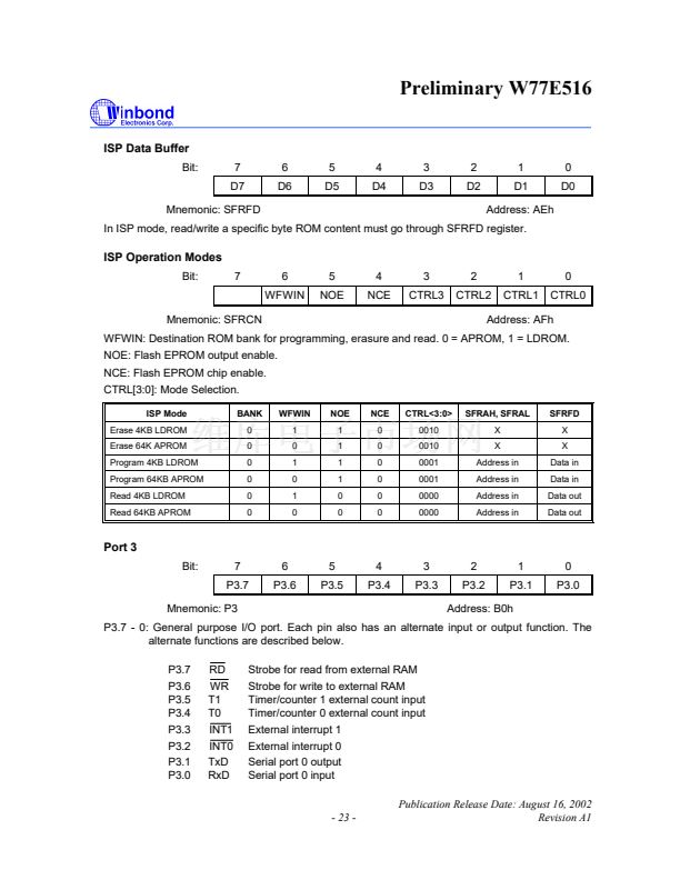
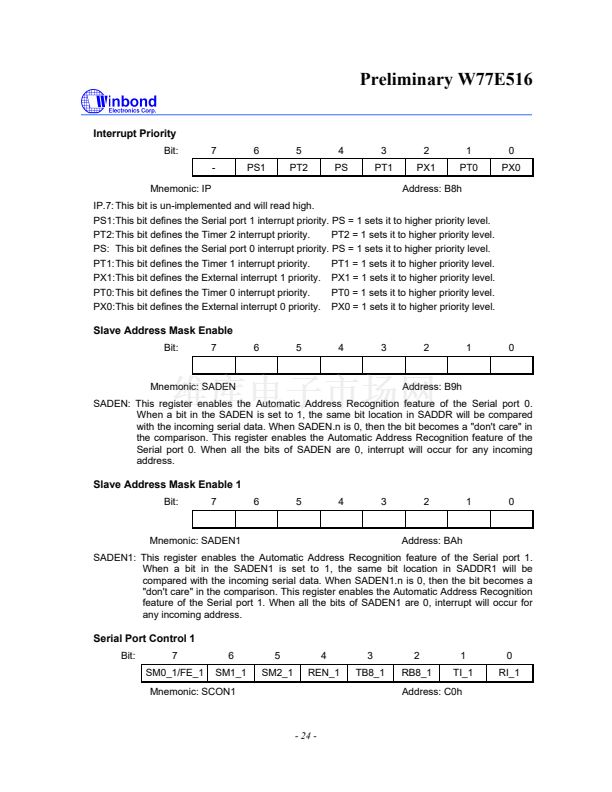
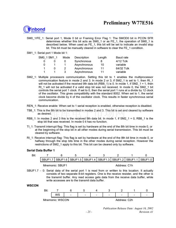
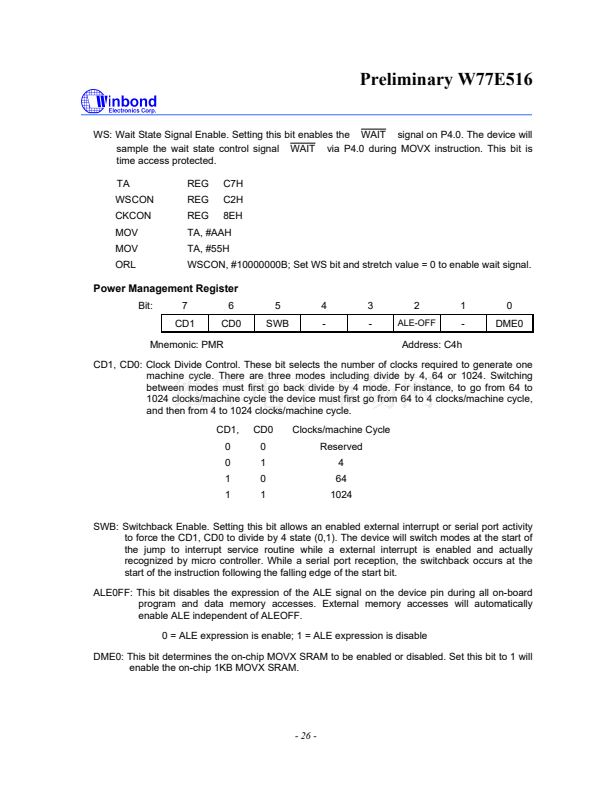
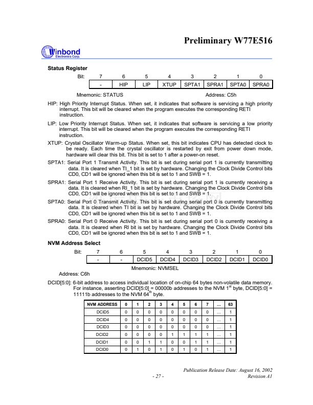
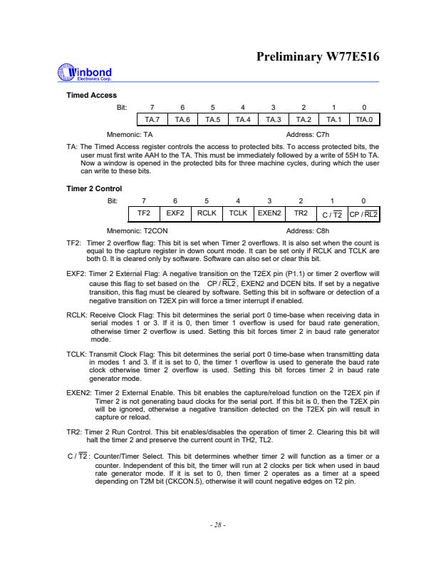
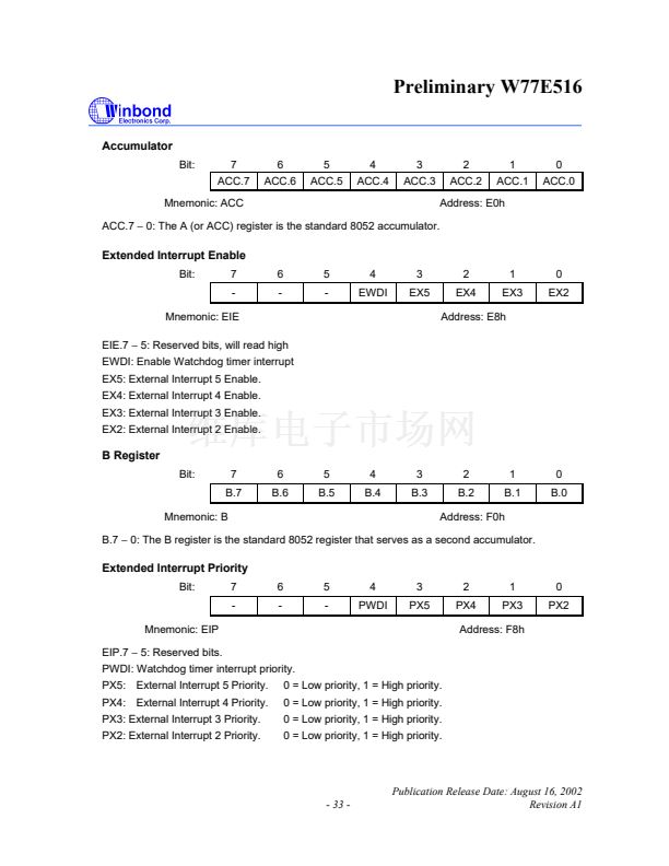
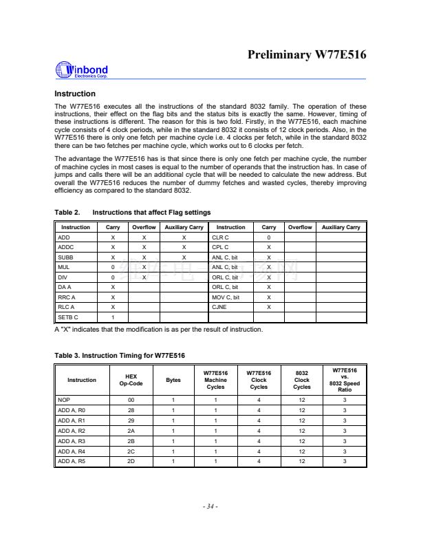
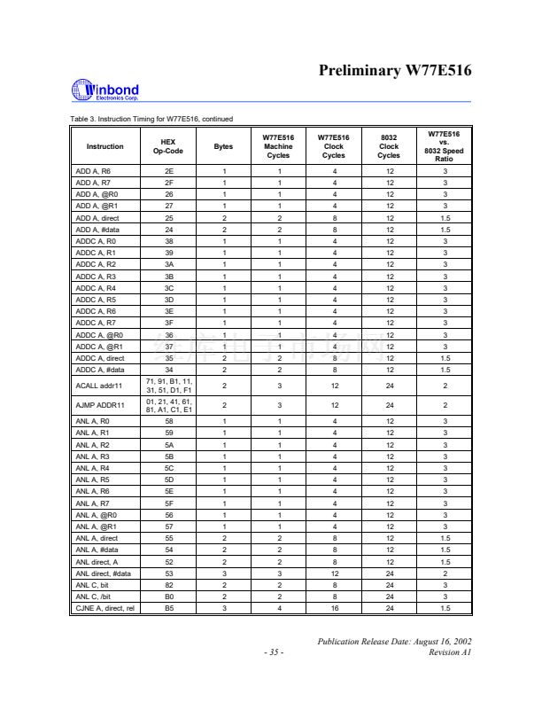
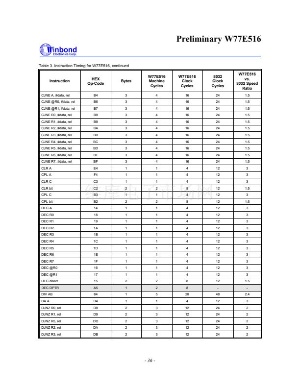
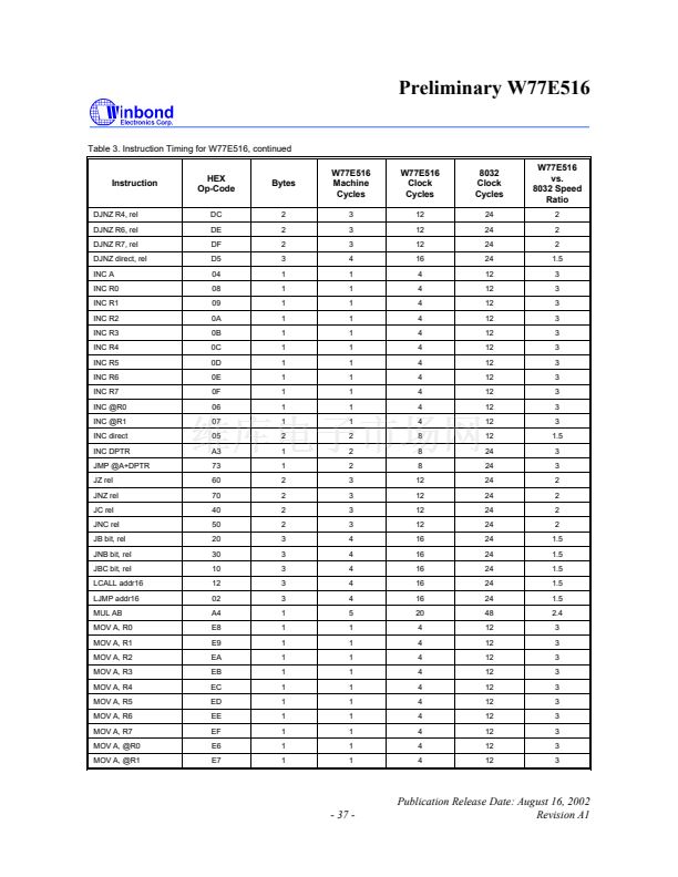
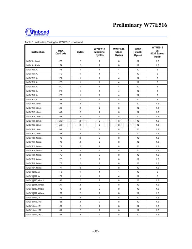
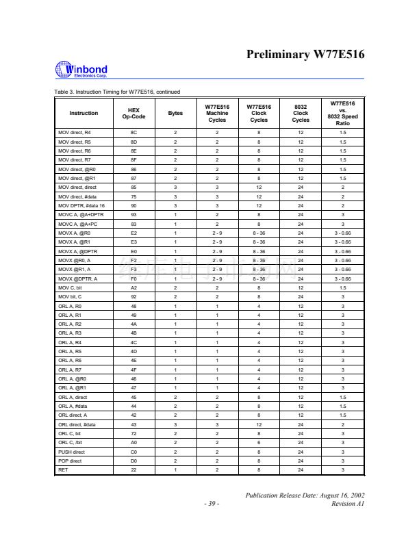
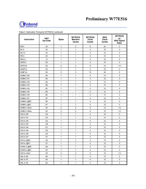
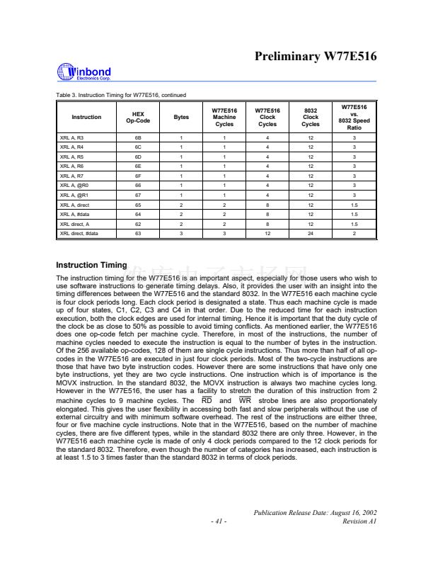
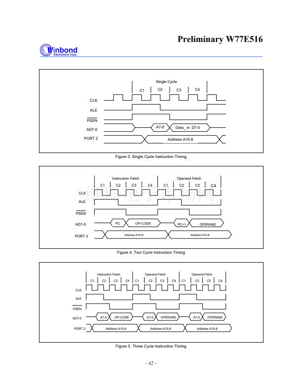
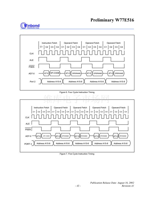
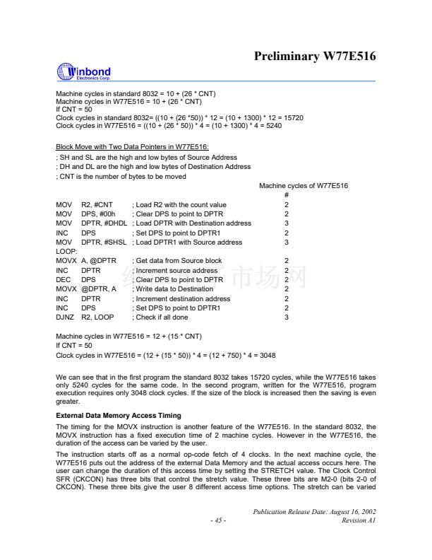
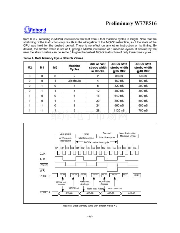
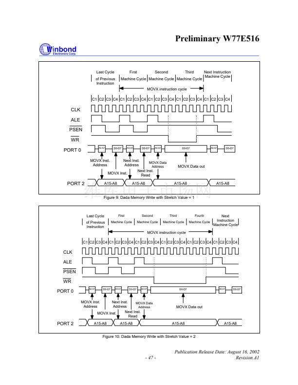
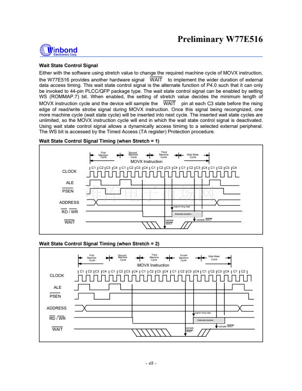
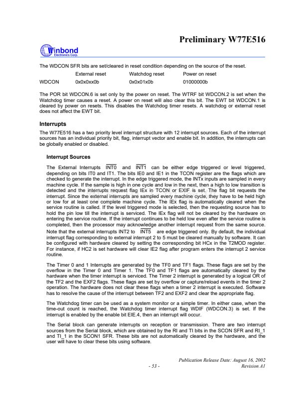
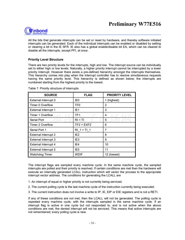
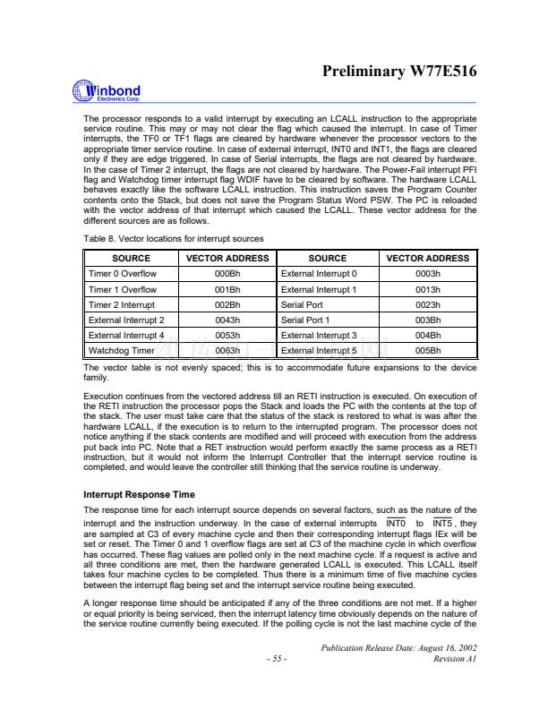
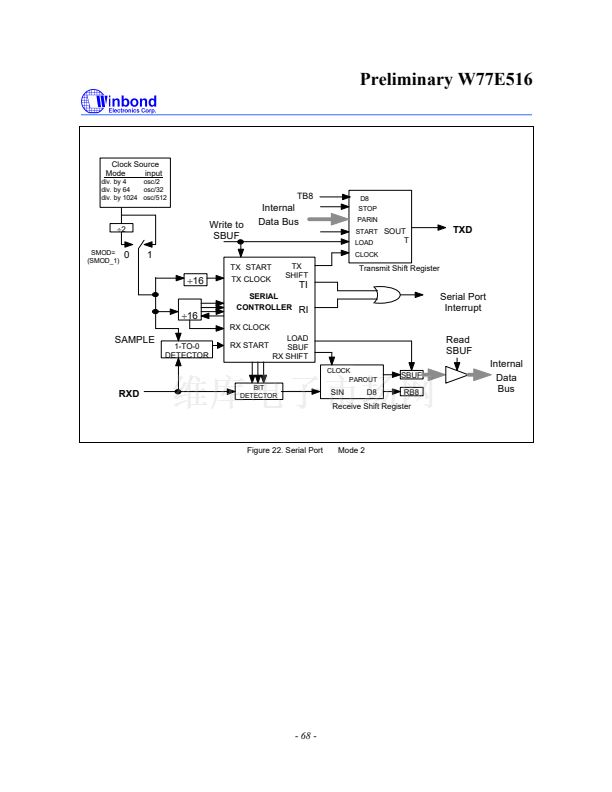
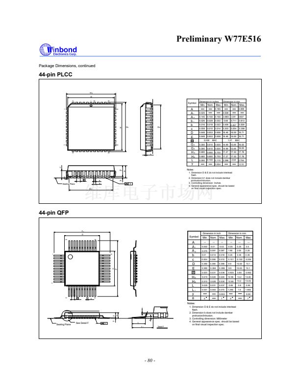
Preliminary W77E516
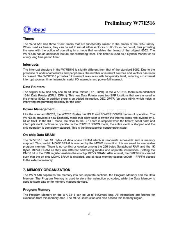
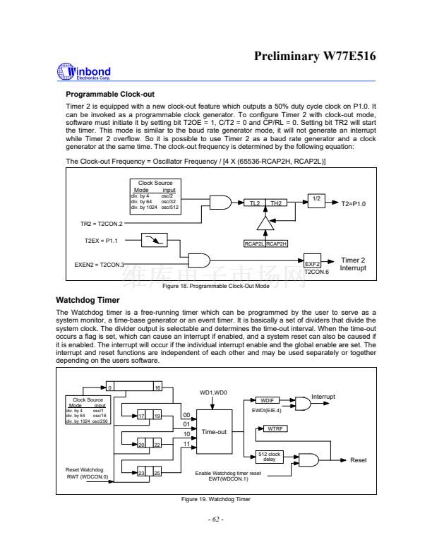
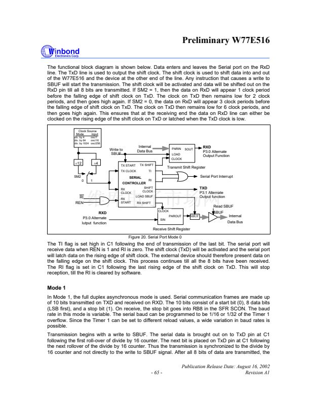
The functional block diagram is shown below. Data enters and leaves the Serial port on the RxD
line. The TxD line is used to output the shift clock. The shift clock is used to shift data into and out
of the W77E516 and the device at the other end of the line. Any instruction that causes a write to
SBUF will start the transmission. The shift clock will be activated and data will be shifted out on the
RxD pin till all 8 bits are transmitted. If SM2 = 1, then the data on RxD will appear 1 clock period
before the falling edge of shift clock on TxD. The clock on TxD then remains low for 2 clock
periods, and then goes high again. If SM2 = 0, the data on RxD will appear 3 clock periods before
the falling edge of shift clock on TxD. The clock on TxD then remains low for 6 clock periods, and
then goes high again. This ensures that at the receiving end the data on RxD line can either be
clocked on the rising edge of the shift clock on TxD or latched when the TxD clock is low.
Clock Source
Mode
input
div. by 4
osc/1
div. by 64
osc/16
div. by 1024 osc/256
Write to
SBUF
梅12
梅4
TX START
TX CLOCK
Internal
Data Bus
PARIN
LOAD
CLOCK
SOUT
RXD
P3.0 Alternate
Output Function
TX SHIFT
TI
Transmit Shift Register
Serial Port Interrupt
SM2
0
1
SERIAL
CONTROLLER
RX
CLOCK
RI
SHIFT
CLOCK
RI
REN
RXD
P3.0 Alternate
Iutput function
RX
START
LOAD SBUF
RX SHIFT
TXD
P3.1 Alternate
Output function
Read SBUF
CLOCK
PAROUT
SIN
SBUF
SBUF
Internal
Data Bus
Receive Shift Register
Figure 20. Serial Port Mode 0
The TI flag is set high in C1 following the end of transmission of the last bit. The serial port will
receive data when REN is 1 and RI is zero. The shift clock (TxD) will be activated and the serial port
will latch data on the rising edge of shift clock. The external device should therefore present data on
the falling edge on the shift clock. This process continues till all the 8 bits have been received.
The RI flag is set in C1 following the last rising edge of the shift clock on TxD. This will stop
reception, till the RI is cleared by software.
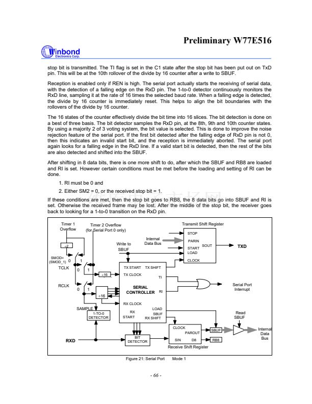
Mode 1
In Mode 1, the full duplex asynchronous mode is used. Serial communication frames are made up
of 10 bits transmitted on TXD and received on RXD. The 10 bits consist of a start bit (0), 8 data bits
(LSB first), and a stop bit (1). On receive, the stop bit goes into RB8 in the SFR SCON. The baud
rate in this mode is variable. The serial baud can be programmed to be 1/16 or 1/32 of the Timer 1
overflow. Since the Timer 1 can be set to different reload values, a wide variation in baud rates is
possible.
Transmission begins with a write to SBUF. The serial data is brought out on to TxD pin at C1
following the first roll-over of divide by 16 counter. The next bit is placed on TxD pin at C1 following
the next rollover of the divide by 16 counter. Thus the transmission is synchronized to the divide by
16 counter and not directly to the write to SBUF signal. After all 8 bits of data are transmitted, the
Publication Release Date: August 16, 2002
Revision A1
- 65 -


 1
1
 2
2
 3
3
 4
4
 5
5
 6
6
 7
7
 8
8
 9
9
 10
10
 11
11
 12
12
 13
13
 14
14
 15
15
 16
16
 17
17
 18
18
 19
19
 20
20
 21
21
 22
22
 23
23
 24
24
 25
25
 26
26
 27
27
 28
28
 29
29
 30
30
 31
31
 32
32
 33
33
 34
34
 35
35
 36
36
 37
37
 38
38
 39
39
 40
40
 41
41
 42
42
 43
43
 44
44
 45
45
 46
46
 47
47
 48
48
 49
49
 50
50
 51
51
 52
52
 53
53
 54
54
 55
55
 56
56
 57
57
 58
58
 59
59
 60
60
 61
61
 62
62
 63
63
 64
64
 65
65
 66
66
 67
67
 68
68
 69
69
 70
70
 71
71
 72
72
 73
73
 74
74
 75
75
 76
76
 77
77
 78
78
 79
79
 80
80
 81
81
 82
82
 83
83
 84
84
 85
85
