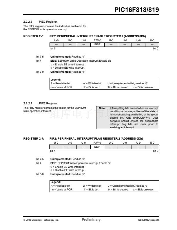
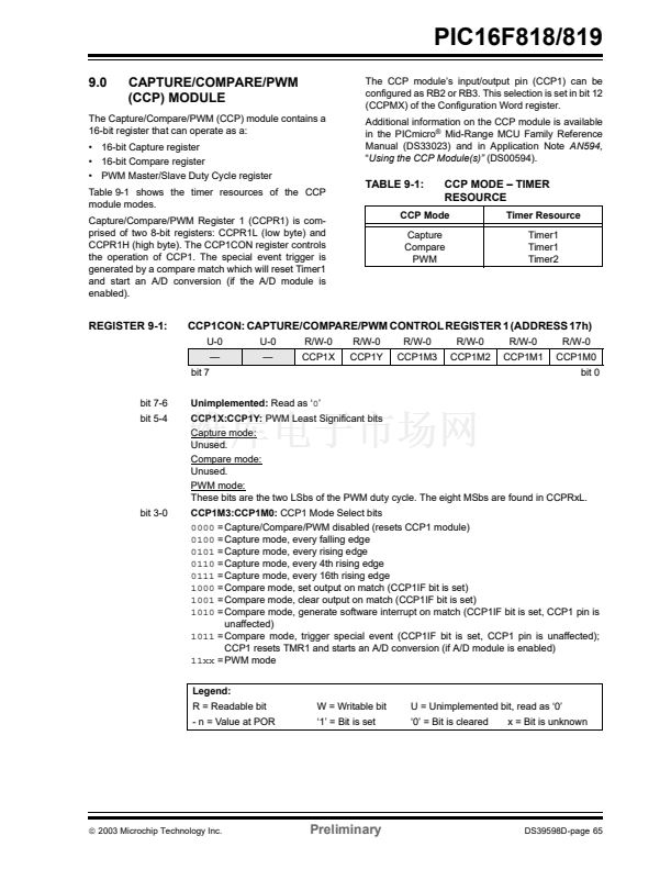
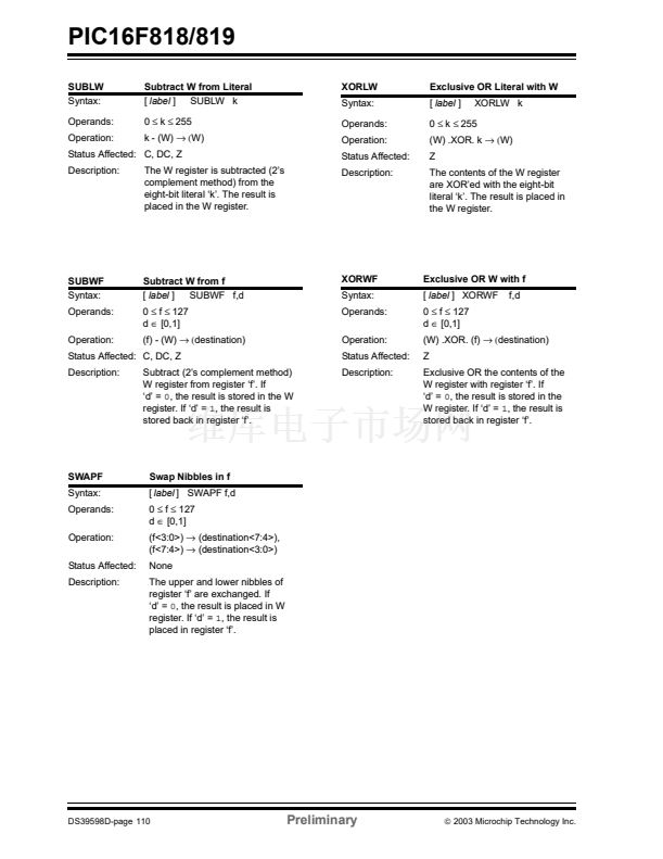
(EECON1<0>). Once the read control bit is set, the
instruction cycle to read the data. This causes the
EECON1, RD鈥?/div>
instruction to be ignored. The data
is available in the very next cycle in the EEDATA and
EEDATH registers; therefore, it can be read as two
bytes in the following instructions. EEDATA and
EEDATH registers will hold this value until another read
or until it is written to by the user (during a write
operation).
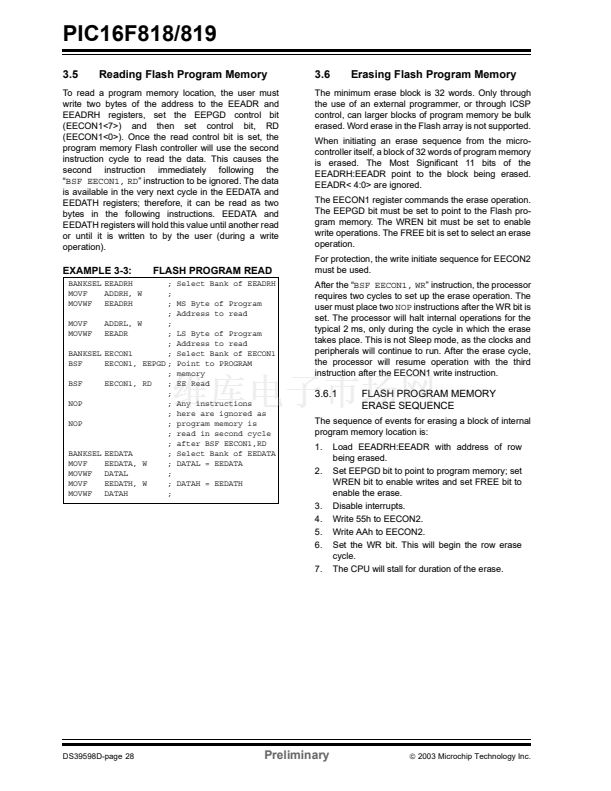
The minimum erase block is 32 words. Only through
the use of an external programmer, or through ICSP
control, can larger blocks of program memory be bulk
erased. Word erase in the Flash array is not supported.
When initiating an erase sequence from the micro-
controller itself, a block of 32 words of program memory
is erased. The Most Significant 11 bits of the
EEADRH:EEADR point to the block being erased.
EEADR< 4:0> are ignored.
The EECON1 register commands the erase operation.
The EEPGD bit must be set to point to the Flash pro-
gram memory. The WREN bit must be set to enable
write operations. The FREE bit is set to select an erase
operation.
For protection, the write initiate sequence for EECON2
must be used.
After the 鈥淏SF
EECON1, WR鈥?/div>
instruction, the processor
requires two cycles to set up the erase operation. The
user must place two
NOP
instructions after the WR bit is
set. The processor will halt internal operations for the
typical 2 ms, only during the cycle in which the erase
takes place. This is not Sleep mode, as the clocks and
peripherals will continue to run. After the erase cycle,
the processor will resume operation with the third
instruction after the EECON1 write instruction.
EXAMPLE 3-3:
BANKSEL EEADRH
MOVF
ADDRH, W
MOVWF
EEADRH
FLASH PROGRAM READ
Select Bank of EEADRH
MS Byte of Program
Address to read
LS Byte of Program
Address to read
Select Bank of EECON1
Point to PROGRAM
memory
EE Read
Any instructions
here are ignored as
program memory is
read in second cycle
after BSF EECON1,RD
Select Bank of EEDATA
DATAL = EEDATA
DATAH = EEDATH
;
;
;
;
MOVF
ADDRL, W
;
MOVWF
EEADR
;
;
BANKSEL EECON1
;
BSF
EECON1, EEPGD ;
;
BSF
EECON1, RD
;
;
NOP
;
;
NOP
;
;
;
BANKSEL EEDATA
;
MOVF
EEDATA, W
;
MOVWF
DATAL
;
MOVF
EEDATH, W
;
MOVWF
DATAH
;
3.6.1
FLASH PROGRAM MEMORY
ERASE SEQUENCE
The sequence of events for erasing a block of internal
program memory location is:
1.
2.
Load EEADRH:EEADR with address of row
being erased.
Set EEPGD bit to point to program memory; set
WREN bit to enable writes and set FREE bit to
enable the erase.
Disable interrupts.
Write 55h to EECON2.
Write AAh to EECON2.
Set the WR bit. This will begin the row erase
cycle.
The CPU will stall for duration of the erase.
3.
4.
5.
6.
7.
DS39598D-page 28
Preliminary
铮?/div>
2003 Microchip Technology Inc.


 1
1
 2
2
 3
3
 4
4
 5
5
 6
6
 7
7
 8
8
 9
9
 10
10
 11
11
 12
12
 13
13
 14
14
 15
15
 16
16
 17
17
 18
18
 19
19
 20
20
 21
21
 22
22
 23
23
 24
24
 25
25
 26
26
 27
27
 28
28
 29
29
 30
30
 31
31
 32
32
 33
33
 34
34
 35
35
 36
36
 37
37
 38
38
 39
39
 40
40
 41
41
 42
42
 43
43
 44
44
 45
45
 46
46
 47
47
 48
48
 49
49
 50
50
 51
51
 52
52
 53
53
 54
54
 55
55
 56
56
 57
57
 58
58
 59
59
 60
60
 61
61
 62
62
 63
63
 64
64
 65
65
 66
66
 67
67
 68
68
 69
69
 70
70
 71
71
 72
72
 73
73
 74
74
 75
75
 76
76
 77
77
 78
78
 79
79
 80
80
 81
81
 82
82
 83
83
 84
84
 85
85
 86
86
 87
87
 88
88
 89
89
 90
90
 91
91
 92
92
 93
93
 94
94
 95
95
 96
96
 97
97
 98
98
 99
99
 100
100
 101
101
 102
102
 103
103
 104
104
 105
105
 106
106
 107
107
 108
108
 109
109
 110
110
 111
111
 112
112
 113
113
 114
114
 115
115
 116
116
 117
117
 118
118
 119
119
 120
120
 121
121
 122
122
 123
123
 124
124
 125
125
 126
126
 127
127
 128
128
 129
129
 130
130
 131
131
 132
132
 133
133
 134
134
 135
135
 136
136
 137
137
 138
138
 139
139
 140
140
 141
141
 142
142
 143
143
 144
144
 145
145
 146
146
 147
147
 148
148
 149
149
 150
150
 151
151
 152
152
 153
153
 154
154
 155
155
 156
156
 157
157
 158
158
 159
159
 160
160
 161
161
 162
162
 163
163
 164
164
