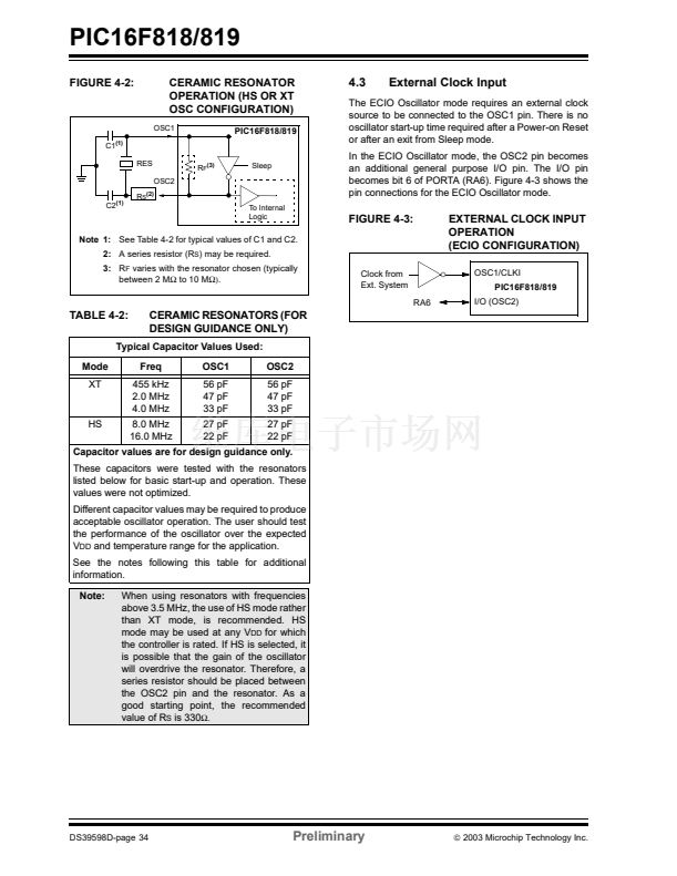
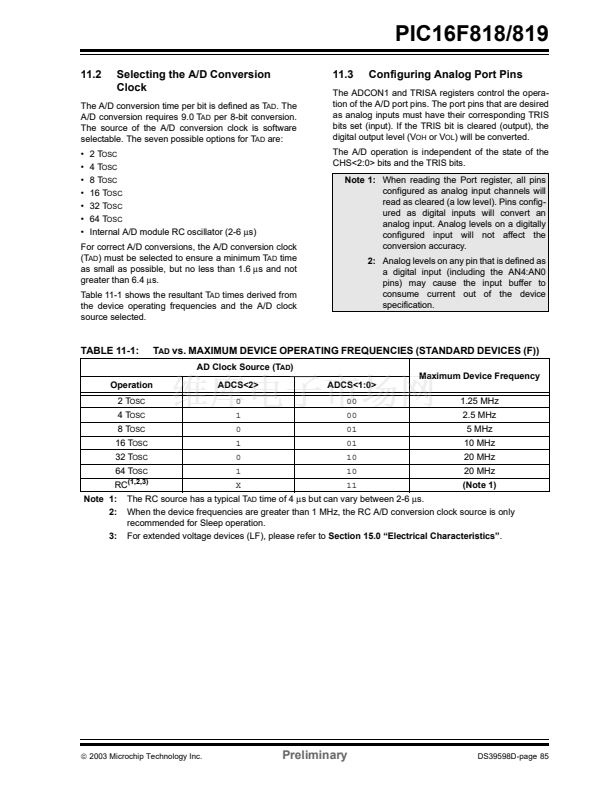
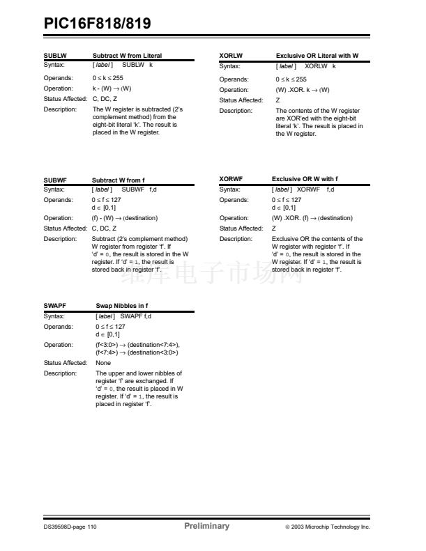
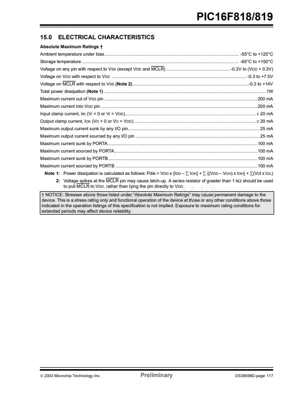
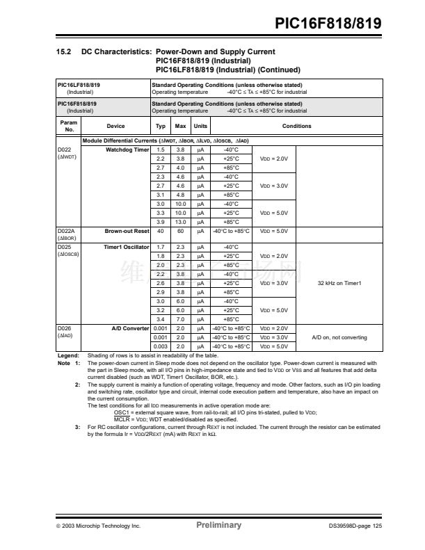
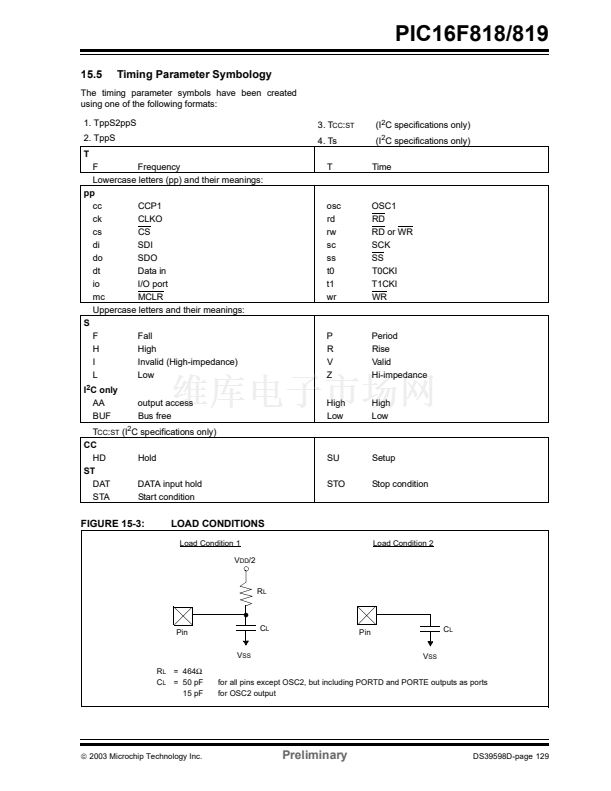
PIC16F818/819
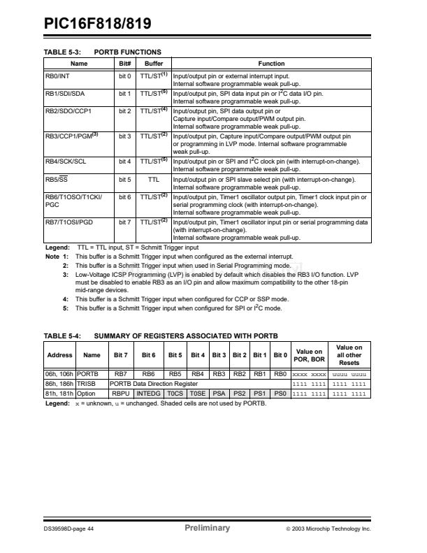
TABLE 5-3:
Name
RB0/INT
RB1/SDI/SDA
RB2/SDO/CCP1
PORTB FUNCTIONS
Bit#
bit 0
bit 1
bit 2
Buffer
Function
TTL/ST
(1)
Input/output pin or external interrupt input.
Internal software programmable weak pull-up.
TTL/ST
(5)
Input/output pin, SPI data input pin or I
2
C data I/O pin.
Internal software programmable weak pull-up.
TTL/ST
(4)
Input/output pin, SPI data output pin or
Capture input/Compare output/PWM output pin.
Internal software programmable weak pull-up.
TTL/ST
(2)
Input/output pin, Capture input/Compare output/PWM output pin
or programming in LVP mode. Internal software programmable
weak pull-up.
TTL/ST
(5)
Input/output pin or SPI and I
2
C clock pin (with interrupt-on-change).
Internal software programmable weak pull-up.
TTL
Input/output pin or SPI slave select pin (with interrupt-on-change).
Internal software programmable weak pull-up.
RB3/CCP1/PGM
(3)
bit 3
RB4/SCK/SCL
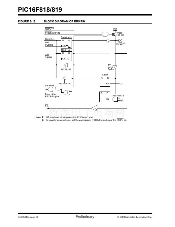
RB5/SS
RB6/T1OSO/T1CKI/
PGC
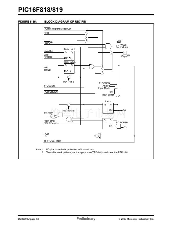
RB7/T1OSI/PGD
bit 4
bit 5
bit 6
TTL/ST
(2)
Input/output pin, Timer1 oscillator output pin, Timer1 clock input pin or
serial programming clock (with interrupt-on-change).
Internal software programmable weak pull-up.
TTL/ST
(2)
Input/output pin, Timer1 oscillator input pin or serial programming data
(with interrupt-on-change).
Internal software programmable weak pull-up.
bit 7
Legend:
TTL = TTL input, ST = Schmitt Trigger input
Note 1:
This buffer is a Schmitt Trigger input when configured as the external interrupt.
2:
This buffer is a Schmitt Trigger input when used in Serial Programming mode.
3:
Low-Voltage ICSP Programming (LVP) is enabled by default which disables the RB3 I/O function. LVP
must be disabled to enable RB3 as an I/O pin and allow maximum compatibility to the other 18-pin
mid-range devices.
4:
This buffer is a Schmitt Trigger input when configured for CCP or SSP mode.
5:
This buffer is a Schmitt Trigger input when configured for SPI or I
2
C mode.
TABLE 5-4:
Address
SUMMARY OF REGISTERS ASSOCIATED WITH PORTB
Name
Bit 7
RB7
RBPU
Bit 6
RB6
INTEDG
Bit 5
RB5
T0CS
Bit 4
RB4
T0SE
Bit 3
RB3
PSA
Bit 2
RB2
PS2
Bit 1
RB1
PS1
Bit 0
Value on
POR, BOR
Value on
all other
Resets
06h, 106h PORTB
86h, 186h TRISB
81h, 181h Option
RB0
xxxx xxxx uuuu uuuu
1111 1111 1111 1111
PS0
1111 1111 1111 1111
PORTB Data Direction Register
Legend:
x
= unknown,
u
= unchanged. Shaded cells are not used by PORTB.
DS39598D-page 44
Preliminary
铮?/div>
2003 Microchip Technology Inc.


 1
1
 2
2
 3
3
 4
4
 5
5
 6
6
 7
7
 8
8
 9
9
 10
10
 11
11
 12
12
 13
13
 14
14
 15
15
 16
16
 17
17
 18
18
 19
19
 20
20
 21
21
 22
22
 23
23
 24
24
 25
25
 26
26
 27
27
 28
28
 29
29
 30
30
 31
31
 32
32
 33
33
 34
34
 35
35
 36
36
 37
37
 38
38
 39
39
 40
40
 41
41
 42
42
 43
43
 44
44
 45
45
 46
46
 47
47
 48
48
 49
49
 50
50
 51
51
 52
52
 53
53
 54
54
 55
55
 56
56
 57
57
 58
58
 59
59
 60
60
 61
61
 62
62
 63
63
 64
64
 65
65
 66
66
 67
67
 68
68
 69
69
 70
70
 71
71
 72
72
 73
73
 74
74
 75
75
 76
76
 77
77
 78
78
 79
79
 80
80
 81
81
 82
82
 83
83
 84
84
 85
85
 86
86
 87
87
 88
88
 89
89
 90
90
 91
91
 92
92
 93
93
 94
94
 95
95
 96
96
 97
97
 98
98
 99
99
 100
100
 101
101
 102
102
 103
103
 104
104
 105
105
 106
106
 107
107
 108
108
 109
109
 110
110
 111
111
 112
112
 113
113
 114
114
 115
115
 116
116
 117
117
 118
118
 119
119
 120
120
 121
121
 122
122
 123
123
 124
124
 125
125
 126
126
 127
127
 128
128
 129
129
 130
130
 131
131
 132
132
 133
133
 134
134
 135
135
 136
136
 137
137
 138
138
 139
139
 140
140
 141
141
 142
142
 143
143
 144
144
 145
145
 146
146
 147
147
 148
148
 149
149
 150
150
 151
151
 152
152
 153
153
 154
154
 155
155
 156
156
 157
157
 158
158
 159
159
 160
160
 161
161
 162
162
 163
163
 164
164
