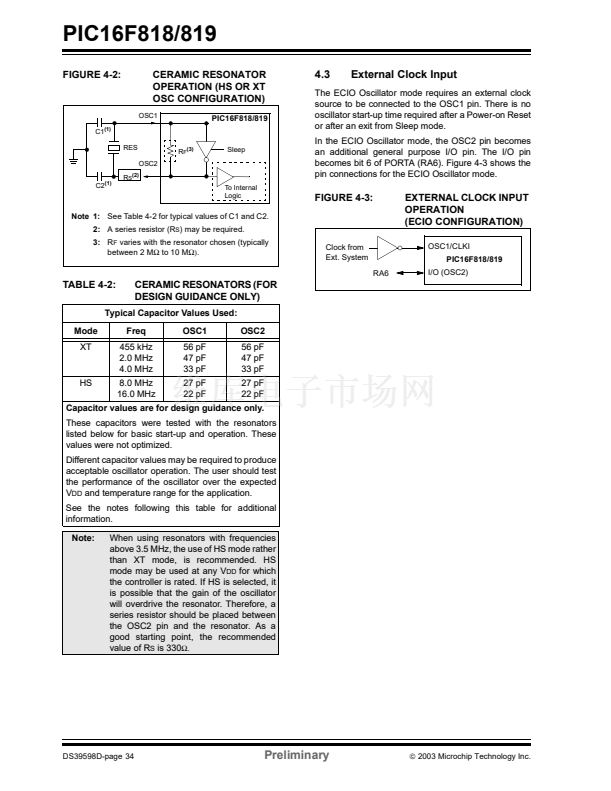
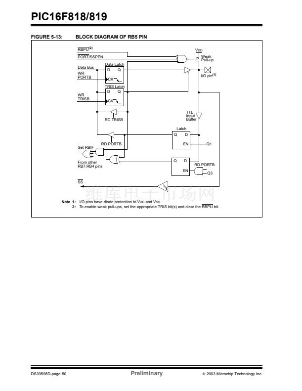
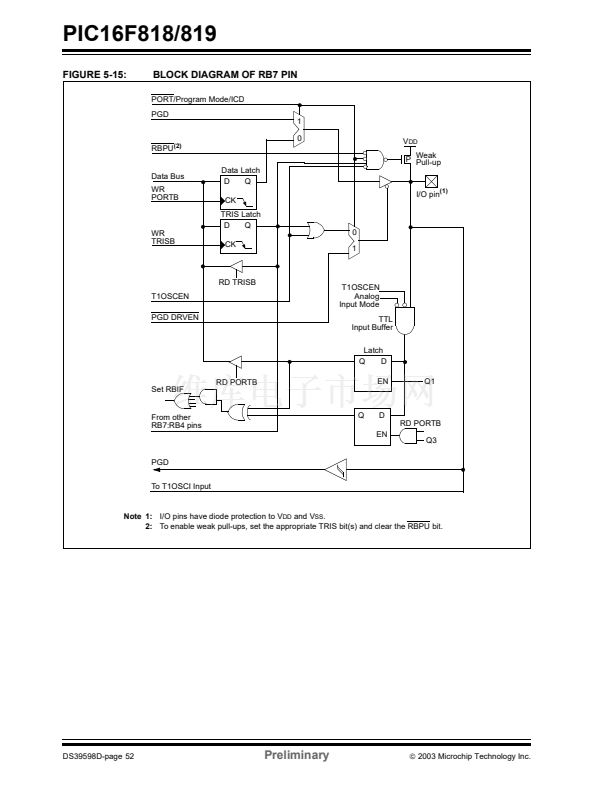
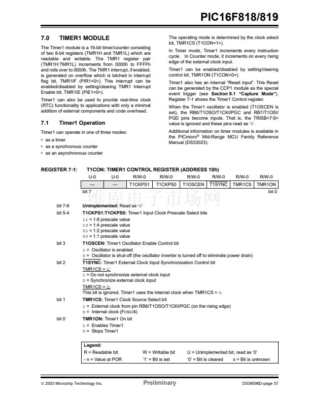
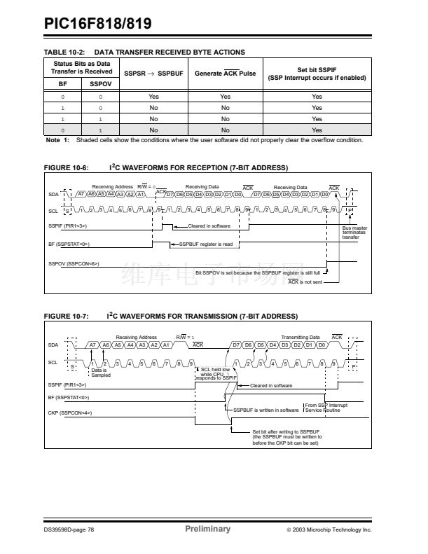
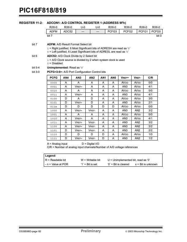
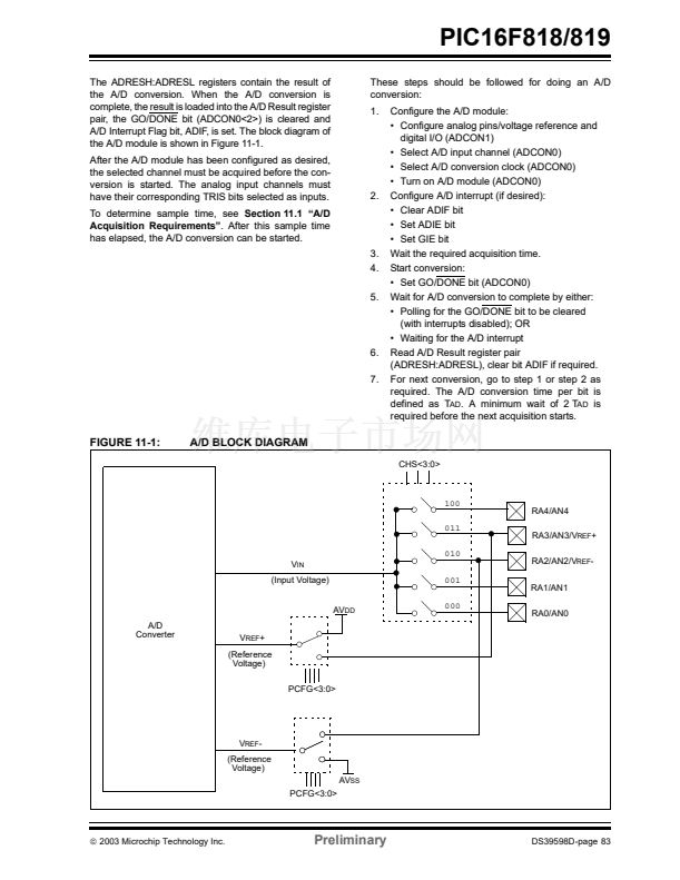
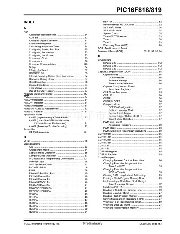
PIC16F818/819
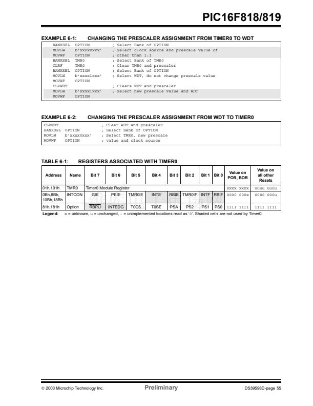
EXAMPLE 6-1:
BANKSEL
MOVLW
MOVWF
BANKSEL
CLRF
BANKSEL
MOVLW
MOVWF
CLRWDT
MOVLW
MOVWF
CHANGING THE PRESCALER ASSIGNMENT FROM TIMER0 TO WDT
;
;
;
;
;
;
;
Select Bank of OPTION
Select clock source and prescale value of
other than 1:1
Select Bank of TMR0
Clear TMR0 and prescaler
Select Bank of OPTION
Select WDT, do not change prescale value
OPTION
b'xx0x0xxx'
OPTION
TMR0
TMR0
OPTION
b'xxxx1xxx'
OPTION
b'xxxx1xxx'
OPTION
; Clears WDT and prescaler
; Select new prescale value and WDT
EXAMPLE 6-2:
CHANGING THE PRESCALER ASSIGNMENT FROM WDT TO TIMER0
;
;
;
;
Clear WDT and prescaler
Select Bank of OPTION
Select TMR0, new prescale
value and clock source
CLRWDT
BANKSEL OPTION
MOVLW
b'xxxx0xxx'
MOVWF
OPTION
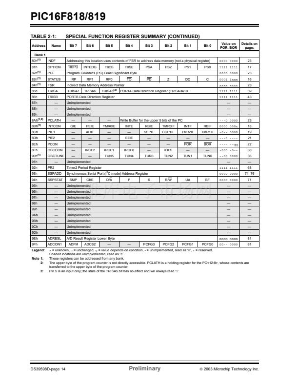
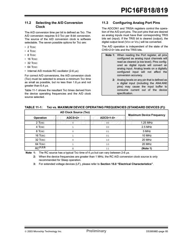
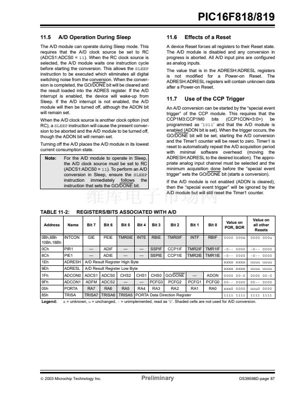
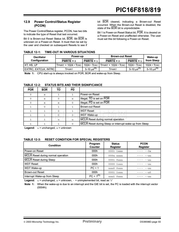
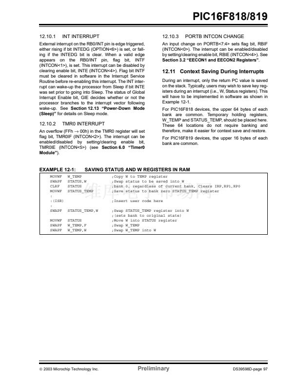
TABLE 6-1:
Address
01h,101h
REGISTERS ASSOCIATED WITH TIMER0
Name
Bit 7
Bit 6
Bit 5
Bit 4
Bit 3
Bit 2
Bit 1
Bit 0
Value on
POR, BOR
xxxx xxxx
INTE
T0SE
RBIE TMR0IF INTF RBIF
0000 000x
PSA
PS2
PS1
PS0
1111 1111
Value on
all other
Resets
uuuu uuuu
0000 000u
1111 1111
TMR0
Timer0 Module Register
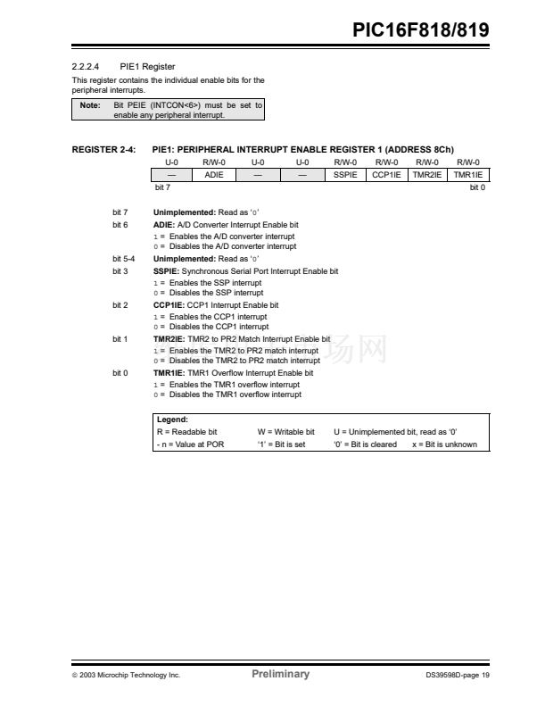
GIE
RBPU
PEIE
INTEDG
TMR0IE
T0CS
0Bh,8Bh,
INTCON
10Bh,18Bh
81h,181h
Legend:
Option
x
= unknown,
u
= unchanged,
-
= unimplemented locations read as 鈥?鈥? Shaded cells are not used by Timer0.
铮?/div>
2003 Microchip Technology Inc.
Preliminary
DS39598D-page 55


 1
1
 2
2
 3
3
 4
4
 5
5
 6
6
 7
7
 8
8
 9
9
 10
10
 11
11
 12
12
 13
13
 14
14
 15
15
 16
16
 17
17
 18
18
 19
19
 20
20
 21
21
 22
22
 23
23
 24
24
 25
25
 26
26
 27
27
 28
28
 29
29
 30
30
 31
31
 32
32
 33
33
 34
34
 35
35
 36
36
 37
37
 38
38
 39
39
 40
40
 41
41
 42
42
 43
43
 44
44
 45
45
 46
46
 47
47
 48
48
 49
49
 50
50
 51
51
 52
52
 53
53
 54
54
 55
55
 56
56
 57
57
 58
58
 59
59
 60
60
 61
61
 62
62
 63
63
 64
64
 65
65
 66
66
 67
67
 68
68
 69
69
 70
70
 71
71
 72
72
 73
73
 74
74
 75
75
 76
76
 77
77
 78
78
 79
79
 80
80
 81
81
 82
82
 83
83
 84
84
 85
85
 86
86
 87
87
 88
88
 89
89
 90
90
 91
91
 92
92
 93
93
 94
94
 95
95
 96
96
 97
97
 98
98
 99
99
 100
100
 101
101
 102
102
 103
103
 104
104
 105
105
 106
106
 107
107
 108
108
 109
109
 110
110
 111
111
 112
112
 113
113
 114
114
 115
115
 116
116
 117
117
 118
118
 119
119
 120
120
 121
121
 122
122
 123
123
 124
124
 125
125
 126
126
 127
127
 128
128
 129
129
 130
130
 131
131
 132
132
 133
133
 134
134
 135
135
 136
136
 137
137
 138
138
 139
139
 140
140
 141
141
 142
142
 143
143
 144
144
 145
145
 146
146
 147
147
 148
148
 149
149
 150
150
 151
151
 152
152
 153
153
 154
154
 155
155
 156
156
 157
157
 158
158
 159
159
 160
160
 161
161
 162
162
 163
163
 164
164
