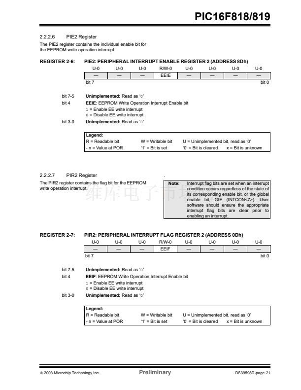
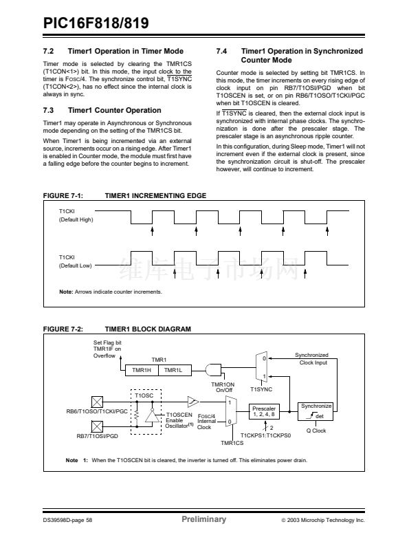
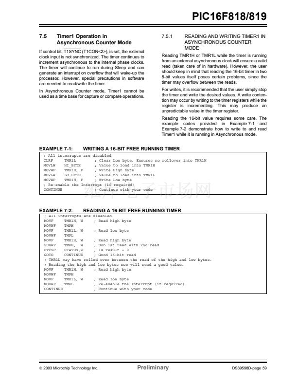
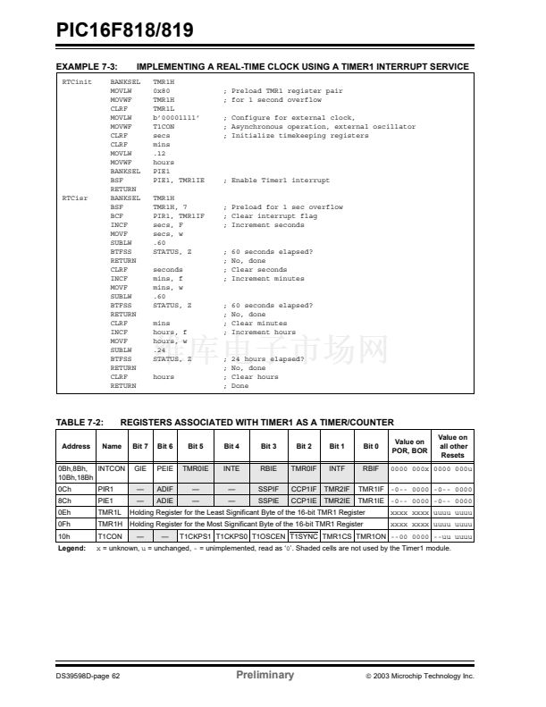
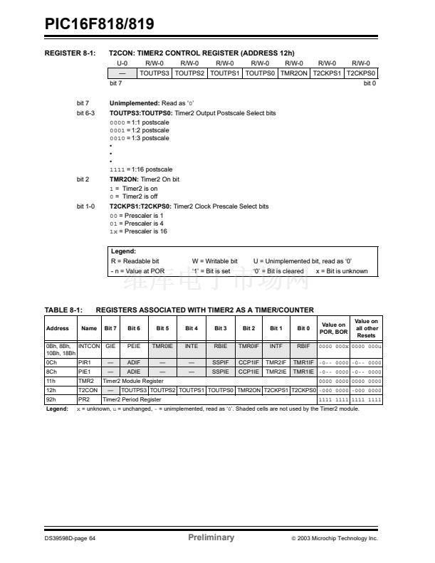
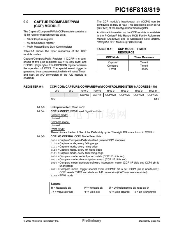
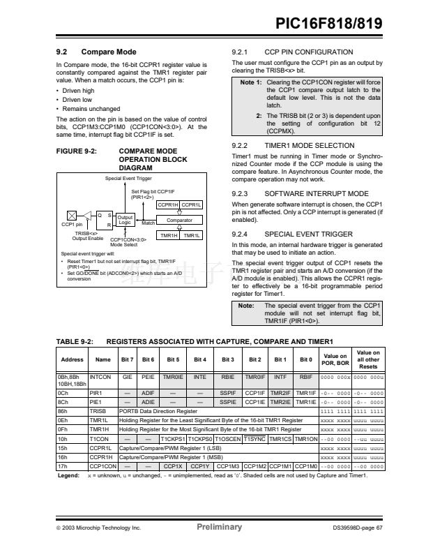
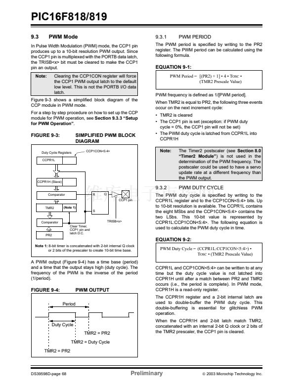
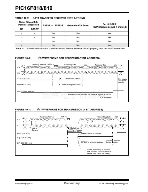
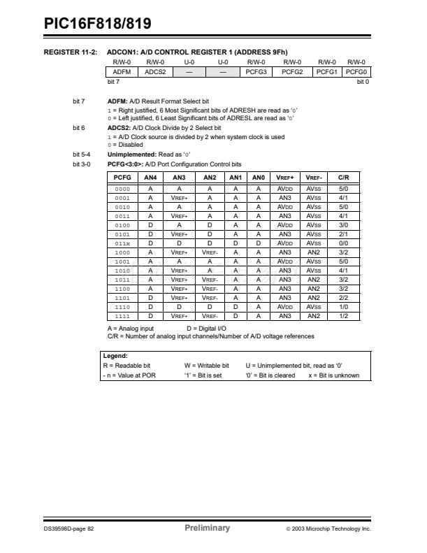
PIC16F818/819
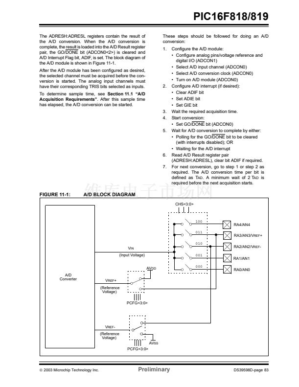
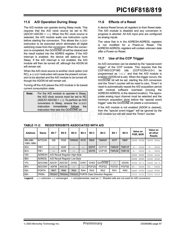
The ADRESH:ADRESL registers contain the result of
the A/D conversion. When the A/D conversion is
complete, the result is loaded into the A/D Result register
pair, the GO/DONE bit (ADCON0<2>) is cleared and
A/D Interrupt Flag bit, ADIF, is set. The block diagram of
the A/D module is shown in Figure 11-1.
After the A/D module has been configured as desired,
the selected channel must be acquired before the con-
version is started. The analog input channels must
have their corresponding TRIS bits selected as inputs.
To determine sample time, see
Section 11.1 鈥淎/D
Acquisition Requirements鈥?
After this sample time
has elapsed, the A/D conversion can be started.
3.
4.
5.
These steps should be followed for doing an A/D
conversion:
1.
Configure the A/D module:
鈥?Configure analog pins/voltage reference and
digital I/O (ADCON1)
鈥?Select A/D input channel (ADCON0)
鈥?Select A/D conversion clock (ADCON0)
鈥?Turn on A/D module (ADCON0)
Configure A/D interrupt (if desired):
鈥?Clear ADIF bit
鈥?Set ADIE bit
鈥?Set GIE bit
Wait the required acquisition time.
Start conversion:
鈥?Set GO/DONE bit (ADCON0)
Wait for A/D conversion to complete by either:
鈥?Polling for the GO/DONE bit to be cleared
(with interrupts disabled); OR
鈥?Waiting for the A/D interrupt
Read A/D Result register pair
(ADRESH:ADRESL), clear bit ADIF if required.
For next conversion, go to step 1 or step 2 as
required. The A/D conversion time per bit is
defined as T
AD
. A minimum wait of 2 T
AD
is
required before the next acquisition starts.
2.
6.
7.
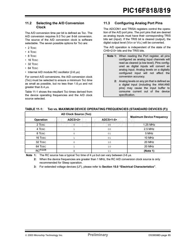
FIGURE 11-1:
A/D BLOCK DIAGRAM
CHS<3:0>
100
RA4/AN4
011
RA3/AN3/V
REF
+
010
V
IN
(Input Voltage)
AV
DD
A/D
Converter
V
REF
+
(Reference
Voltage)
PCFG<3:0>
001
RA1/AN1
000
RA0/AN0
RA2/AN2/V
REF
-
V
REF
-
(Reference
Voltage)
AV
SS
PCFG<3:0>
铮?/div>
2003 Microchip Technology Inc.
Preliminary
DS39598D-page 83


 1
1
 2
2
 3
3
 4
4
 5
5
 6
6
 7
7
 8
8
 9
9
 10
10
 11
11
 12
12
 13
13
 14
14
 15
15
 16
16
 17
17
 18
18
 19
19
 20
20
 21
21
 22
22
 23
23
 24
24
 25
25
 26
26
 27
27
 28
28
 29
29
 30
30
 31
31
 32
32
 33
33
 34
34
 35
35
 36
36
 37
37
 38
38
 39
39
 40
40
 41
41
 42
42
 43
43
 44
44
 45
45
 46
46
 47
47
 48
48
 49
49
 50
50
 51
51
 52
52
 53
53
 54
54
 55
55
 56
56
 57
57
 58
58
 59
59
 60
60
 61
61
 62
62
 63
63
 64
64
 65
65
 66
66
 67
67
 68
68
 69
69
 70
70
 71
71
 72
72
 73
73
 74
74
 75
75
 76
76
 77
77
 78
78
 79
79
 80
80
 81
81
 82
82
 83
83
 84
84
 85
85
 86
86
 87
87
 88
88
 89
89
 90
90
 91
91
 92
92
 93
93
 94
94
 95
95
 96
96
 97
97
 98
98
 99
99
 100
100
 101
101
 102
102
 103
103
 104
104
 105
105
 106
106
 107
107
 108
108
 109
109
 110
110
 111
111
 112
112
 113
113
 114
114
 115
115
 116
116
 117
117
 118
118
 119
119
 120
120
 121
121
 122
122
 123
123
 124
124
 125
125
 126
126
 127
127
 128
128
 129
129
 130
130
 131
131
 132
132
 133
133
 134
134
 135
135
 136
136
 137
137
 138
138
 139
139
 140
140
 141
141
 142
142
 143
143
 144
144
 145
145
 146
146
 147
147
 148
148
 149
149
 150
150
 151
151
 152
152
 153
153
 154
154
 155
155
 156
156
 157
157
 158
158
 159
159
 160
160
 161
161
 162
162
 163
163
 164
164
