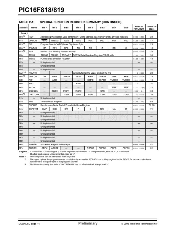
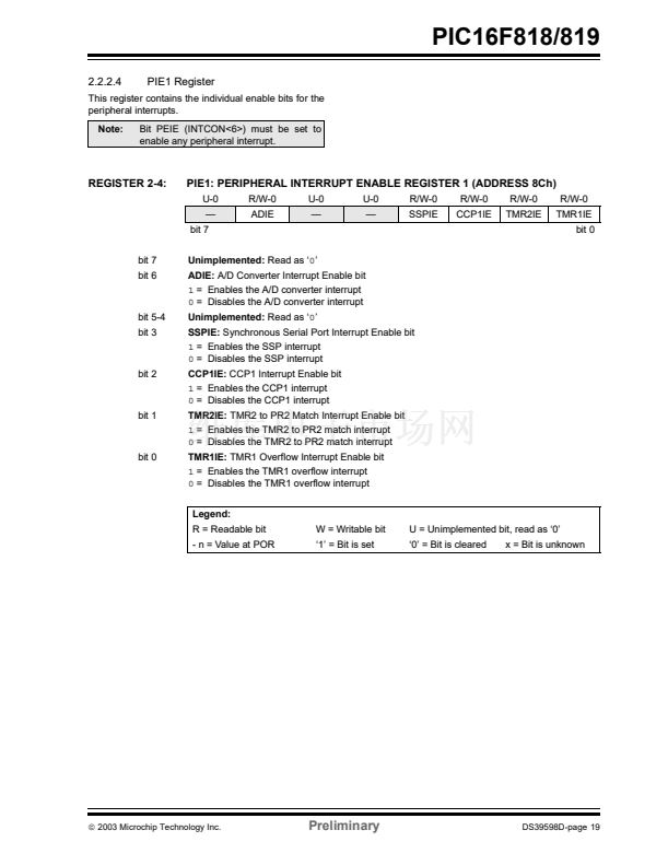
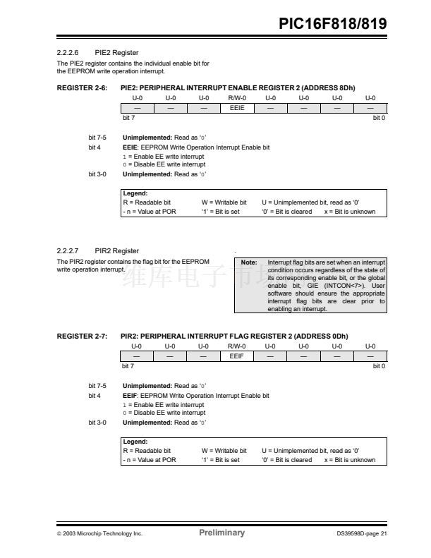
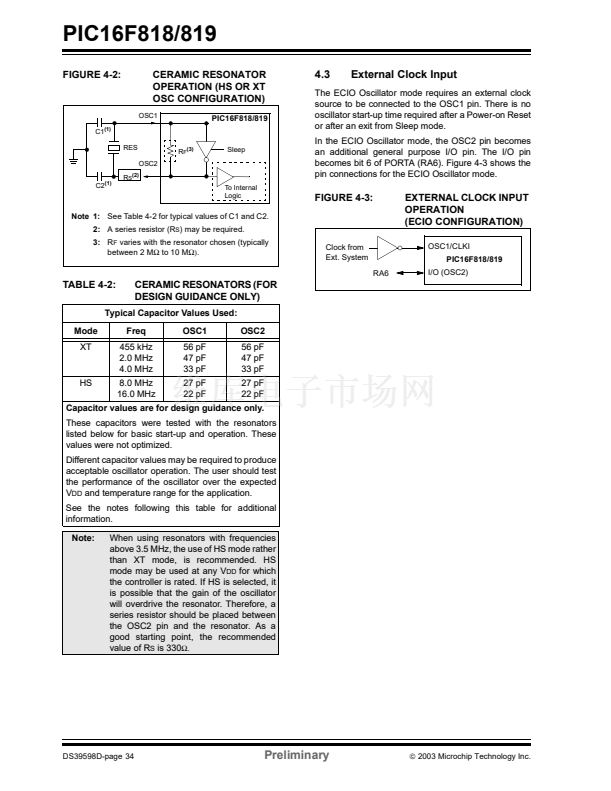
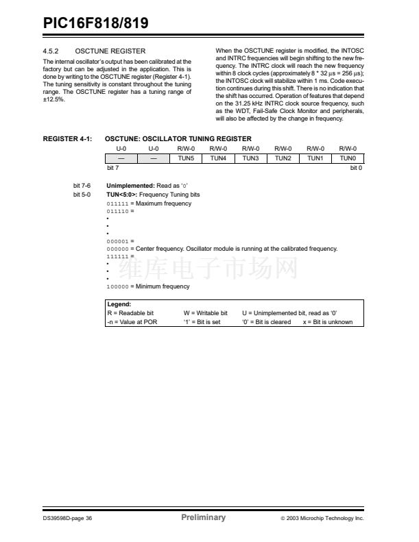
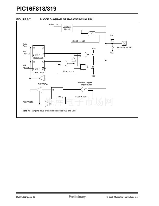
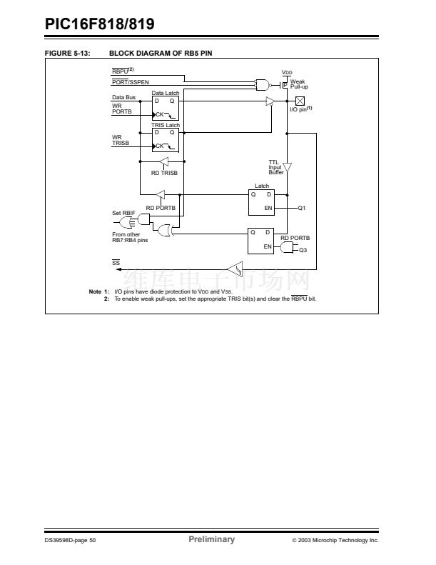
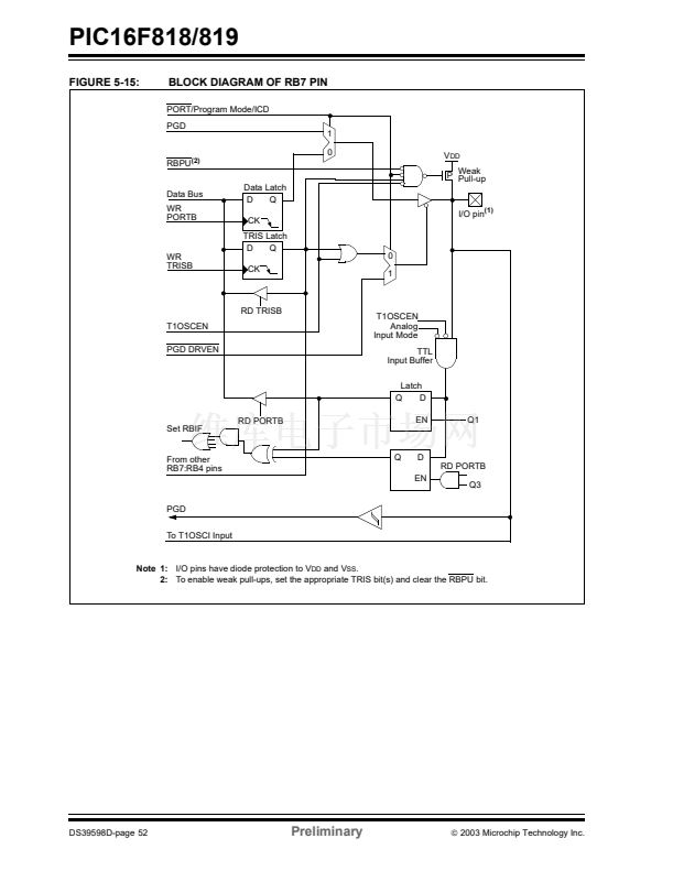
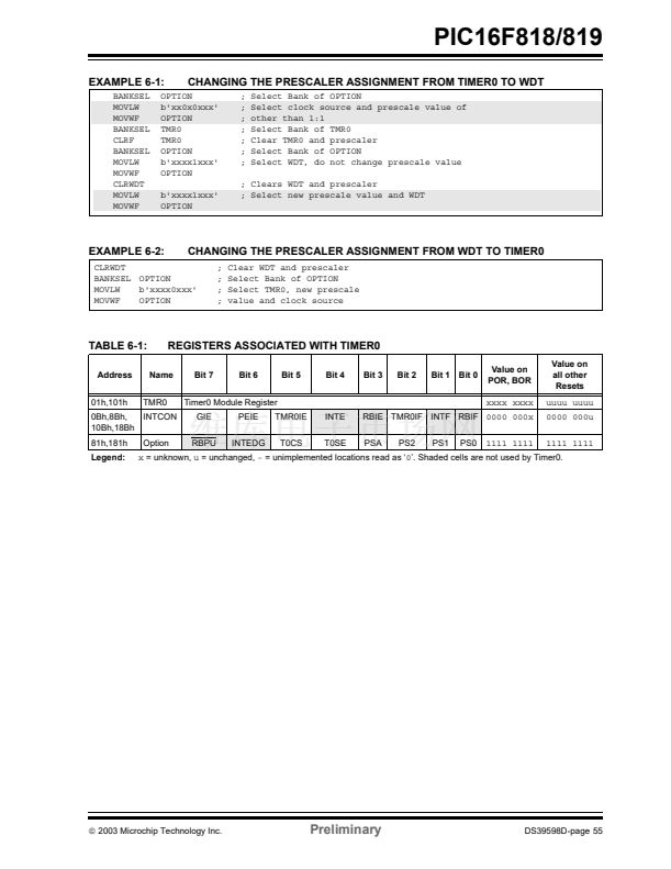
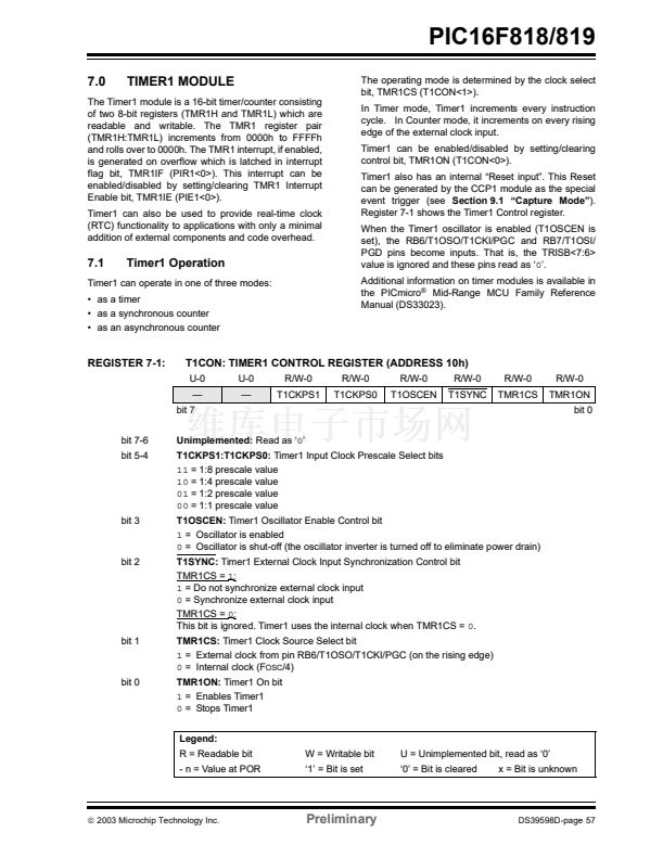
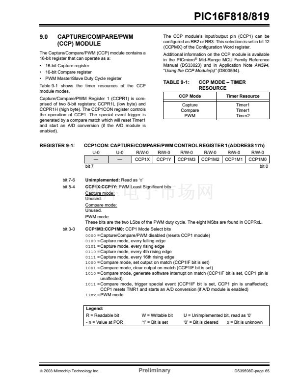
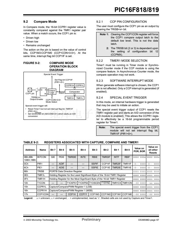
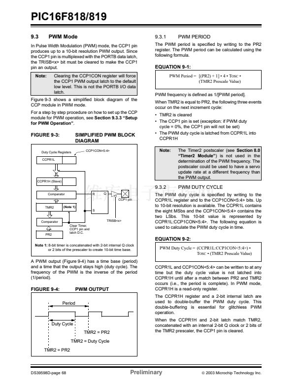
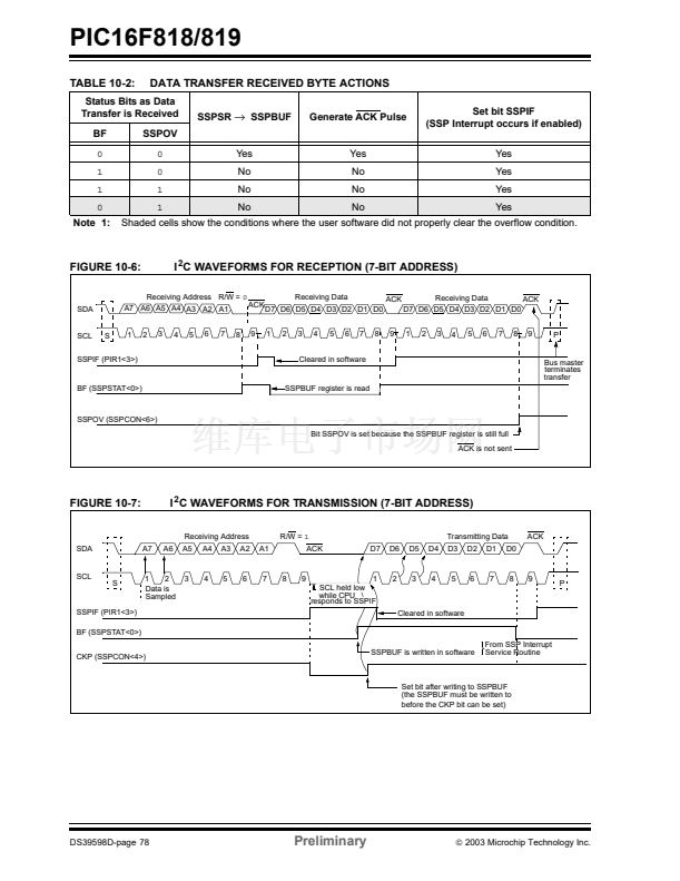
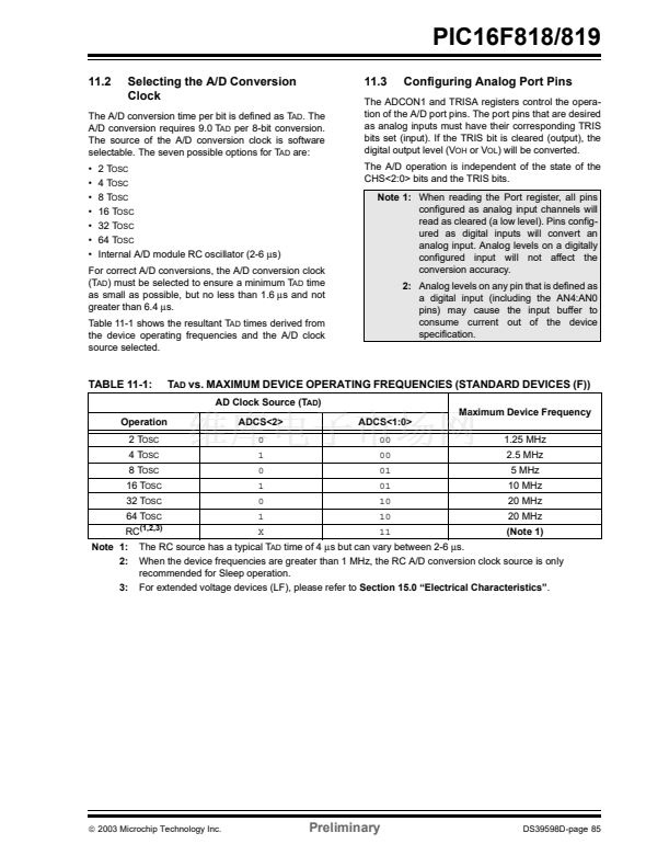
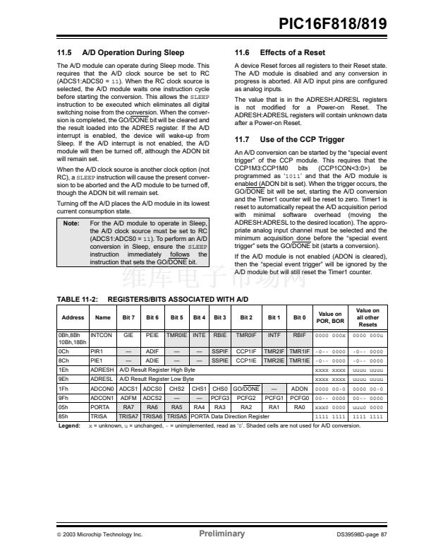
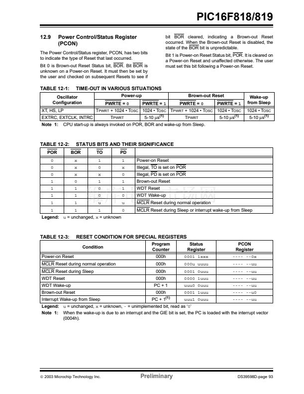
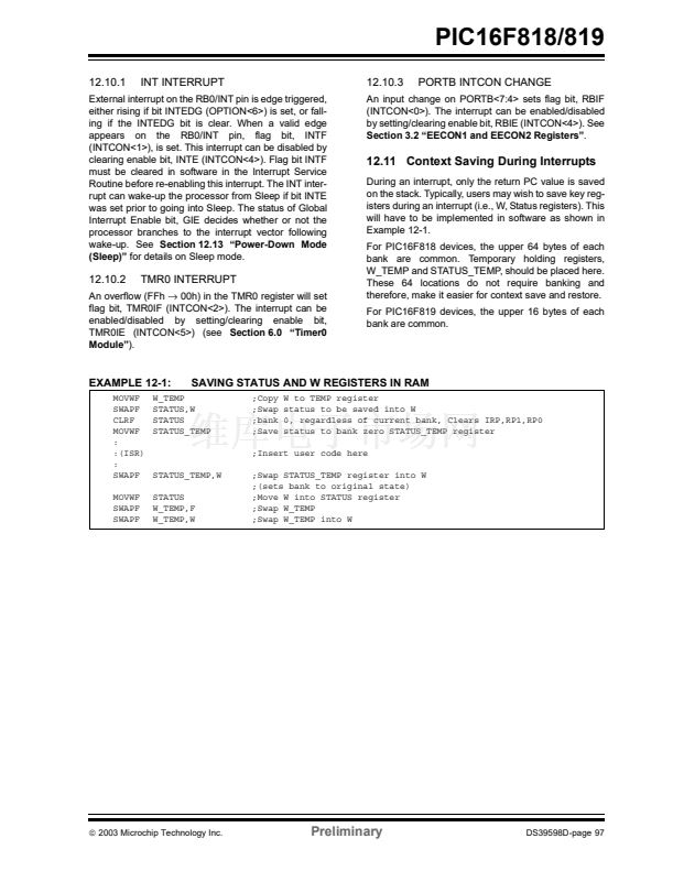
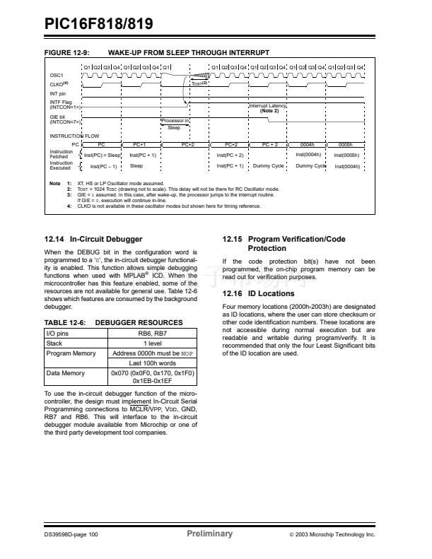
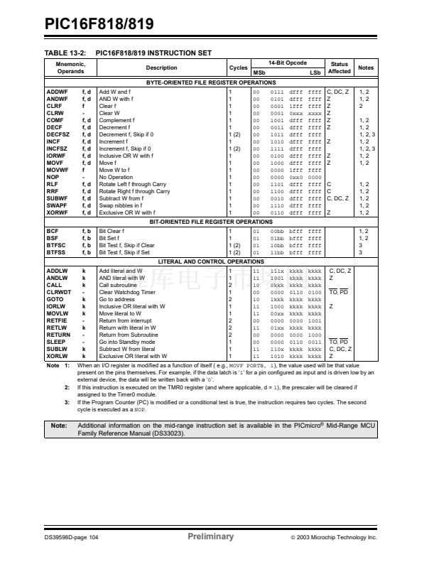
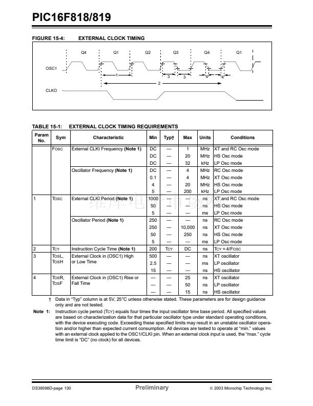
PIC16F818/819
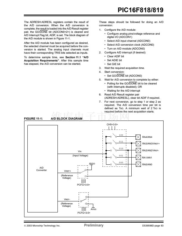
11.1
A/D Acquisition Requirements
For the A/D converter to meet its specified accuracy,
the charge holding capacitor (C
HOLD
) must be allowed
to fully charge to the input channel voltage level. The
analog input model is shown in Figure 11-2. The source
impedance (R
S
) and the internal sampling switch (R
SS
)
impedance directly affect the time required to charge
the capacitor C
HOLD
. The sampling switch (R
SS
)
impedance varies over the device voltage (V
DD
), see
Figure 11-2.
The maximum recommended imped-
ance for analog sources is 2.5 k鈩?
As the impedance
is decreased, the acquisition time may be decreased.
After the analog input channel is selected (changed),
this acquisition must be done before the conversion
can be started.
To calculate the minimum acquisition time,
Equation 11-1 may be used. This equation assumes
that 1/2 LSb error is used (1024 steps for the A/D). The
1/2 LSb error is the maximum error allowed for the A/D
to meet its specified resolution.
To calculate the minimum acquisition time, T
ACQ
, see
the PICmicro
庐
Mid-Range MCU Family Reference
Manual (DS33023).
EQUATION 11-1:
T
ACQ
ACQUISITION TIME
=
Amplifier Settling Time + Hold Capacitor Charging Time + Temperature Coefficient
=
=
=
=
=
=
=
T
AMP
+ T
C
+ T
COFF
2
碌s
+ T
C
+ [(Temperature -25掳C)(0.05
碌s/掳C)]
C
HOLD
(R
IC
+ R
SS
+ R
S
) In(1/2047)
-120 pF (1 k鈩?+ 7 k鈩?+ 10 k鈩? In(0.0004885)
16.47
碌s
2
碌s
+ 16.47
碌s
+ [(50掳C 鈥?25掳C)(0.05
碌s/掳C)
19.72
碌s
T
C
T
ACQ
Note 1:
The reference voltage (V
REF
) has no effect on the equation since it cancels itself out.
2:
The charge holding capacitor (C
HOLD
) is not discharged after each conversion.
3:
The maximum recommended impedance for analog sources is 10 k鈩? This is required to meet the pin
leakage specification.
4:
After a conversion has completed, a 2.0 T
AD
delay must complete before acquisition can begin again.
During this time, the holding capacitor is not connected to the selected A/D input channel.
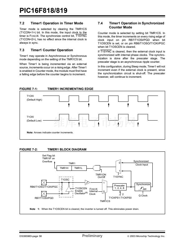
FIGURE 11-2:
ANALOG INPUT MODEL
V
DD
V
T
= 0.6V
R
IC
鈮?/div>
1k
Sampling
Switch
SS
R
SS
C
HOLD
= DAC Capacitance
= 51.2 pF
V
SS
Legend:
C
PIN
= input capacitance
V
T
= threshold voltage
I
LEAKAGE
= leakage current at the pin due to
various junctions
R
IC
= interconnect resistance
SS
= sampling switch
C
HOLD
= sample/hold capacitance (from DAC)
Rs
ANx
VA
C
PIN
5 pF
V
T
= 0.6V
I
LEAKAGE
卤
500 nA
V
DD
6V
5V
4V
3V
2V
5 6 7 8 9 10 11
Sampling Switch
(k鈩?
DS39598D-page 84
Preliminary
铮?/div>
2003 Microchip Technology Inc.


 1
1
 2
2
 3
3
 4
4
 5
5
 6
6
 7
7
 8
8
 9
9
 10
10
 11
11
 12
12
 13
13
 14
14
 15
15
 16
16
 17
17
 18
18
 19
19
 20
20
 21
21
 22
22
 23
23
 24
24
 25
25
 26
26
 27
27
 28
28
 29
29
 30
30
 31
31
 32
32
 33
33
 34
34
 35
35
 36
36
 37
37
 38
38
 39
39
 40
40
 41
41
 42
42
 43
43
 44
44
 45
45
 46
46
 47
47
 48
48
 49
49
 50
50
 51
51
 52
52
 53
53
 54
54
 55
55
 56
56
 57
57
 58
58
 59
59
 60
60
 61
61
 62
62
 63
63
 64
64
 65
65
 66
66
 67
67
 68
68
 69
69
 70
70
 71
71
 72
72
 73
73
 74
74
 75
75
 76
76
 77
77
 78
78
 79
79
 80
80
 81
81
 82
82
 83
83
 84
84
 85
85
 86
86
 87
87
 88
88
 89
89
 90
90
 91
91
 92
92
 93
93
 94
94
 95
95
 96
96
 97
97
 98
98
 99
99
 100
100
 101
101
 102
102
 103
103
 104
104
 105
105
 106
106
 107
107
 108
108
 109
109
 110
110
 111
111
 112
112
 113
113
 114
114
 115
115
 116
116
 117
117
 118
118
 119
119
 120
120
 121
121
 122
122
 123
123
 124
124
 125
125
 126
126
 127
127
 128
128
 129
129
 130
130
 131
131
 132
132
 133
133
 134
134
 135
135
 136
136
 137
137
 138
138
 139
139
 140
140
 141
141
 142
142
 143
143
 144
144
 145
145
 146
146
 147
147
 148
148
 149
149
 150
150
 151
151
 152
152
 153
153
 154
154
 155
155
 156
156
 157
157
 158
158
 159
159
 160
160
 161
161
 162
162
 163
163
 164
164
