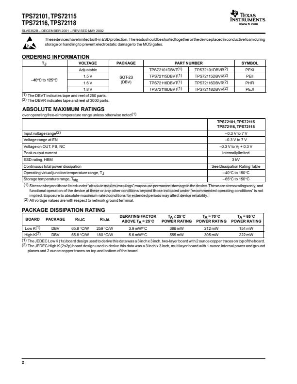
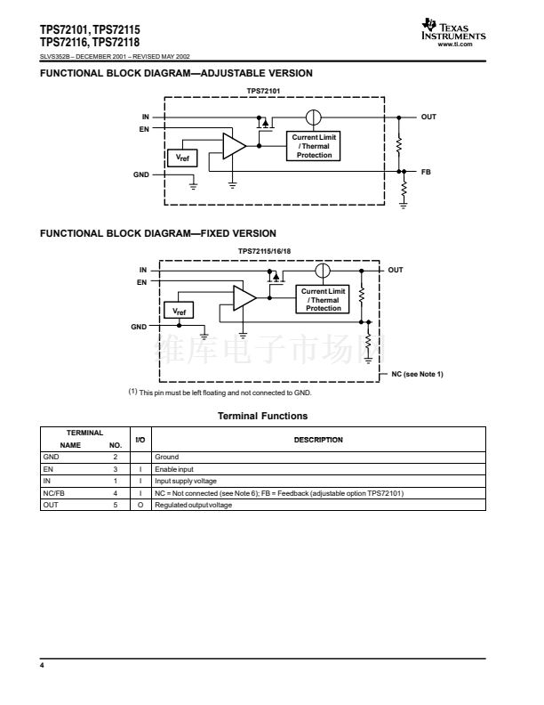
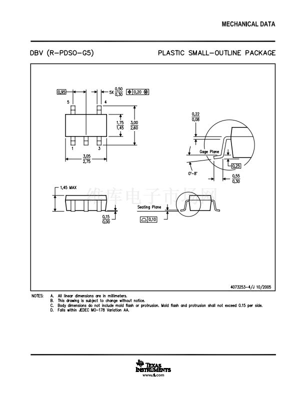
TPS72101, TPS72115
TPS72116, TPS72118
SLVS352B 鈥?DECEMBER 2001 鈥?REVISED MAY 2002
www.ti.com
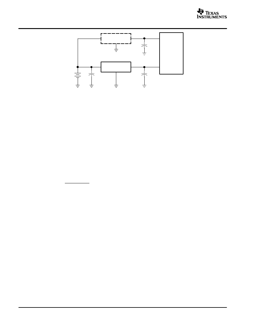
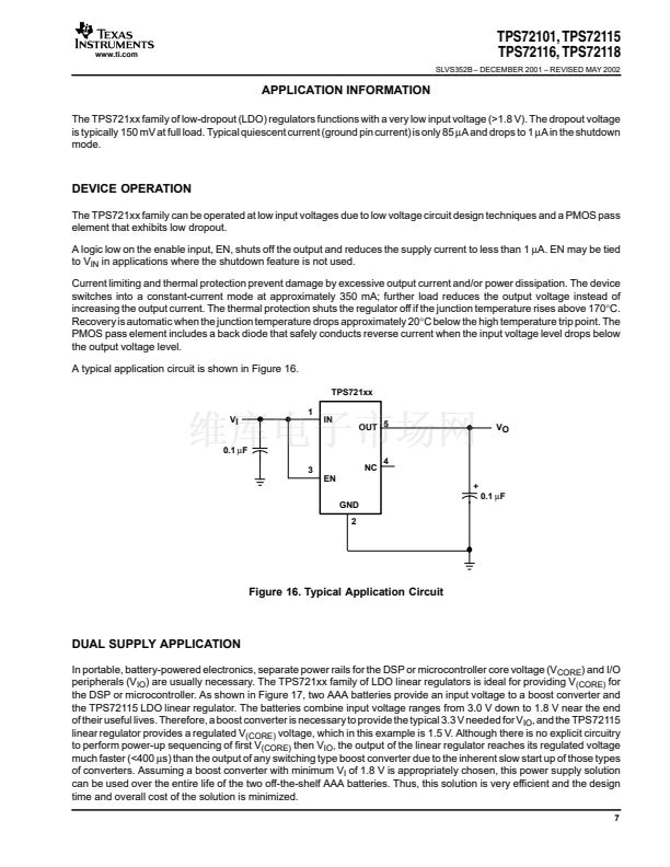
1.8 V 鈥?3 V
3.3 V
Boost Converter
VIO
DSP or
Controller
1.8 V
TPS72115
Two AAA
Batteries
1.5 V
VCORE
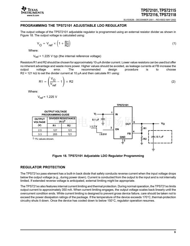
Figure 17. Dual Supply Application Circuit
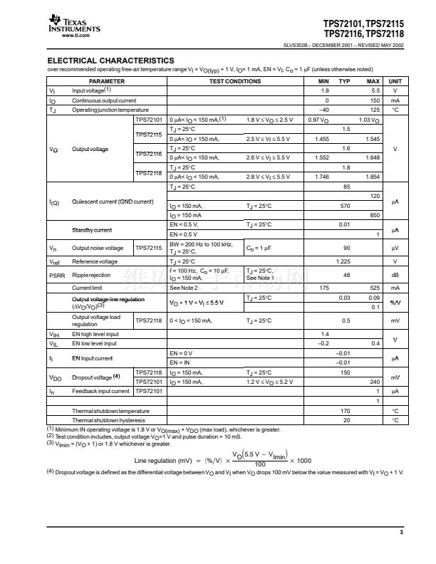
EXTERNAL CAPACITOR REQUIREMENTS
A 0.1-碌F ceramic bypass capacitor is required on both the input and output for stability. Larger capacitors improve transient
response, noise rejection, and ripple rejection. A higher value electrolytic input capacitor may be necessary if large, fast
rise time load transient are anticipated, and/or there is significant input resistance from the device to the input power supply.
POWER DISSIPATION AND JUNCTION TEMPERATURE
Specified regulator operation is assured to a junction temperature of 125掳C; the maximum junction temperature allowable
without damaging the device is 150掳C. This restriction limits the power dissipation the regulator can handle in any given
application. To ensure the junction temperature is within acceptable limits, calculate the maximum allowable dissipation,
P
D(max)
, and the actual dissipation, P
D
, which must be less than or equal to P
D(max)
.
The maximum-power-dissipation limit is determined using the following equation:
T max
*
T
A
P
+
J
D(max)
R
qJA
Where:
T
J
max is the maximum allowable junction temperature.
R
胃JA
is the thermal resistance junction-to-ambient for the package, see the power dissipation rating
table.
T
A
is the ambient temperature.
The regulator dissipation is calculated using:
P
D
+
V
*
V
I
O
I
O
Power dissipation resulting from quiescent current is negligible.
8


 1
1
 2
2
 3
3
 4
4
 5
5
 6
6
 7
7
 8
8
 9
9
 10
10
 11
11
 12
12
 13
13
 14
14
