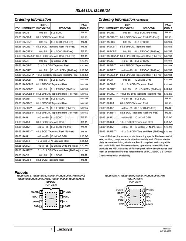
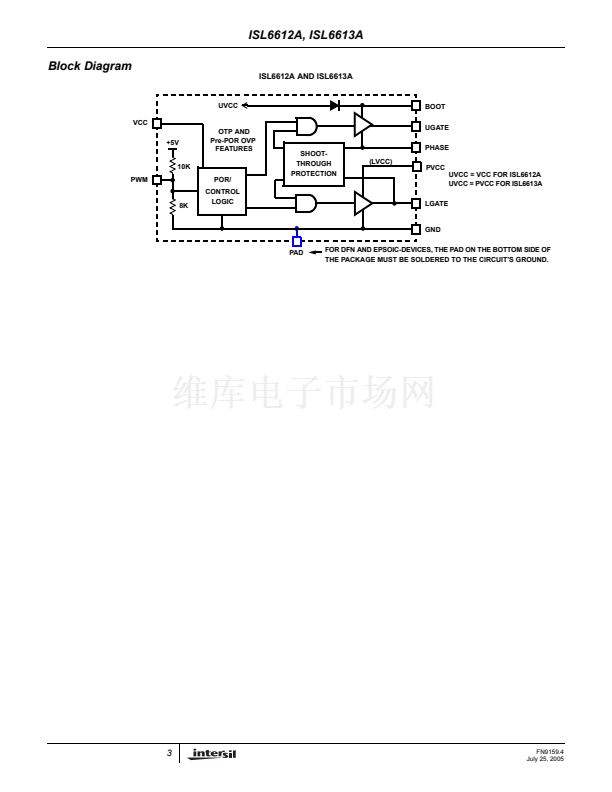
ISL6612A, ISL6613A
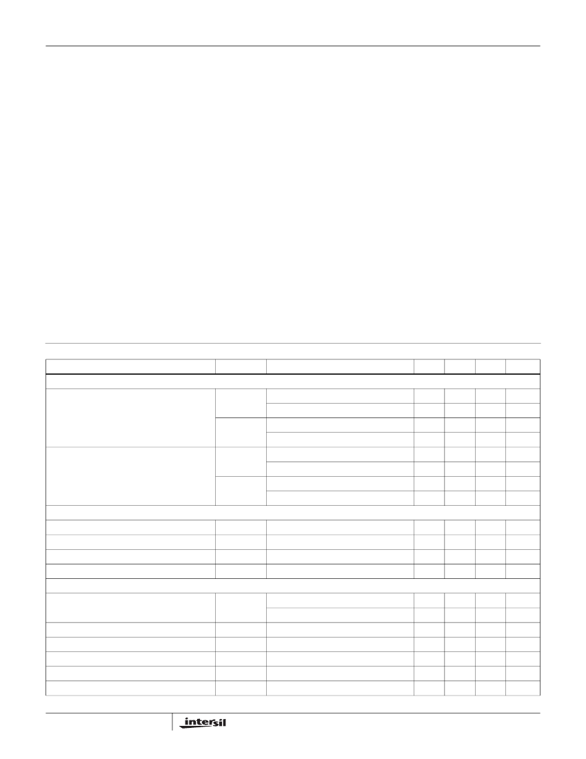
Absolute Maximum Ratings
Supply Voltage (VCC) . . . . . . . . . . . . . . . . . . . . . . . . . . . . . . . . 15V
Supply Voltage (PVCC) . . . . . . . . . . . . . . . . . . . . . . . . . VCC + 0.3V
BOOT Voltage (V
BOOT-GND
) . . . . . . . . . . . . . . . . . . . . . . . . . . . 36V
Input Voltage (V
PWM
). . . . . . . . . . . . . . . . . . . . . . .GND - 0.3V to 7V
UGATE . . . . . . . . . . . . . . . . . . . V
PHASE
- 0.3V
DC
to V
BOOT
+ 0.3V
V
PHASE
- 3.5V (<100ns Pulse Width, 2碌J) to V
BOOT
+ 0.3V
LGATE . . . . . . . . . . . . . . . . . . . . . . GND - 0.3V
DC
to V
PVCC
+ 0.3V
GND - 5V (<100ns Pulse Width, 2碌J) to V
PVCC
+ 0.3V
PHASE . . . . . . . . . . . . . . . . . . . . . . . . . . . . GND - 0.3V
DC
to 15V
DC
GND - 8V (<400ns, 20碌J) to 30V (<200ns, V
BOOT-GND
<36V)
ESD Rating
Human Body Model . . . . . . . . . . . . . . . . . . . .Class I JEDEC STD
Thermal Information
Thermal Resistance
胃
JA
(掳C/W)
胃
JC
(掳C/W)
SOIC Package (Note 1) . . . . . . . . . . . .
100
N/A
EPSOIC Package (Notes 2, 3) . . . . . .
50
7
DFN Package (Notes 2, 3). . . . . . . . . .
48
7
Maximum Junction Temperature (Plastic Package) . . . . . . . . 150掳C
Maximum Storage Temperature Range. . . . . . . . . . . -65掳C to 150掳C
Maximum Lead Temperature (Soldering 10s) . . . . . . . . . . . . . 300掳C
(SOIC - Lead Tips Only)
Recommended Operating Conditions
Ambient Temperature Range . . . . . . . . . . . . . . . . . . . -40掳C to 85掳C
Maximum Operating Junction Temperature . . . . . . . . . . . . . . 125掳C
Supply Voltage, VCC . . . . . . . . . . . . . . . . . . . . . . . . . . . . 12V
卤10%
Supply Voltage Range, PVCC . . . . . . . . . . . . . . . . .5V to 12V
卤10%
CAUTION: Stresses above those listed in 鈥淎bsolute Maximum Ratings鈥?may cause permanent damage to the device. This is a stress only rating and operation of the
device at these or any other conditions above those indicated in the operational sections of this specification is not implied.
NOTES:
1.
胃
JA
is measured with the component mounted on a high effective thermal conductivity test board in free air.
2.
胃
JA
is measured in free air with the component mounted on a high effective thermal conductivity test board with 鈥渄irect attach鈥?features. See Tech
Brief TB379.
3. For
胃
JC
, the 鈥渃ase temp鈥?location is the center of the exposed metal pad on the package underside.
Electrical Specifications
PARAMETER
VCC SUPPLY CURRENT
Bias Supply Current
Recommended Operating Conditions, Unless Otherwise Noted.
SYMBOL
TEST CONDITIONS
MIN
TYP
MAX
UNITS
I
VCC
I
VCC
ISL6612A, f
PWM
= 300kHz, V
VCC
=12V
ISL6613A, f
PWM
= 300kHz, V
VCC
=12V
ISL6612A, f
PWM
= 1MHz, V
VCC
= 12V
ISL6613A, f
PWM
= 1MHz, V
VCC
= 12V
ISL6612A, f
PWM
= 300kHz, V
PVCC
= 12V
ISL6613A, f
PWM
= 300kHz, V
PVCC
= 12V
ISL6612A, f
PWM
= 1MHz, V
PVCC
= 12V
ISL6613A, f
PWM
= 1MHz, V
PVCC
= 12V
-
-
-
-
-
-
-
-
7.2
4.5
11
5
2.5
5.2
7
13
-
-
-
-
-
-
-
-
mA
mA
mA
mA
mA
mA
mA
mA
Gate Drive Bias Current
I
PVCC
I
PVCC
POWER-ON RESET AND ENABLE
VCC Rising Threshold
VCC Rising Threshold
VCC Falling Threshold
VCC Falling Threshold
PWM INPUT (See Timing Diagram on Page 7)
Input Current
I
PWM
V
PWM
= 5V
V
PWM
= 0V
PWM Rising Threshold
PWM Falling Threshold
Typical Three-State Shutdown Window
Three-State Lower Gate Falling Threshold
Three-State Lower Gate Rising Threshold
VCC = 12V
VCC = 12V
VCC = 12V
VCC = 12V
VCC = 12V
-
-
-
-
1.80
-
-
450
-400
3.00
2.00
-
1.50
1.00
-
-
-
-
2.40
-
-
碌A
碌A
V
V
V
V
V
T
A
= 0掳C to 85掳C
T
A
= -40掳C to 85掳C
T
A
= 0掳C to 85掳C
T
A
= -40掳C to 85掳C
9.35
8.35
7.35
6.35
9.80
9.80
7.60
7.60
10.00
10.00
8.00
8.00
V
V
V
V
5
FN9159.4
July 25, 2005


 1
1
 2
2
 3
3
 4
4
 5
5
 6
6
 7
7
 8
8
 9
9
 10
10
 11
11
 12
12
