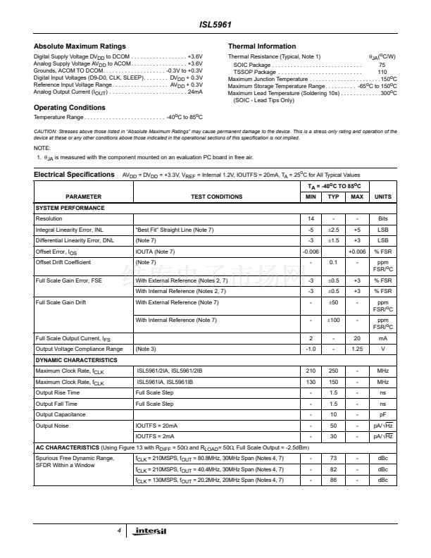
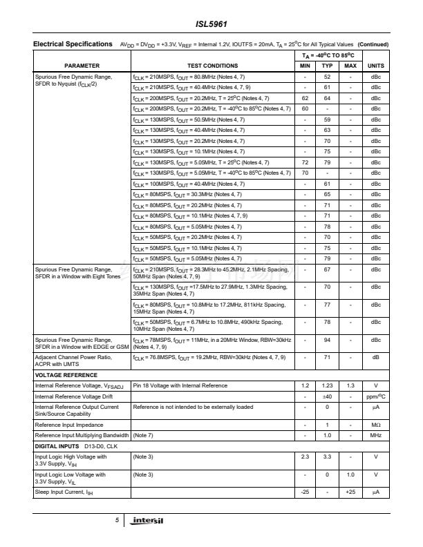
recommended. The allowable supply range is +2.7V to
+3.6V. The recommended supply range is +3.0 to 3.6V
(nominally +3.3V) to maintain optimum SFDR. However,
in SFDR. Reducing the analog output current can help the
SFDR at +2.7V. The SFDR values stated in the table of
specifications were obtained with a +3.3V supply.
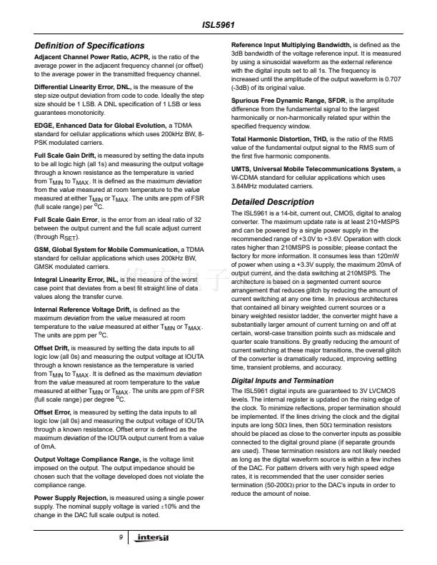
TABLE 1. INPUT CODING vs OUTPUT CURRENT WITH
INTERNAL REFERENCE AND RSET=1.91K鈩?/div>
INPUT CODE (D13-D0)
1111 11111 11111
1000 00000 00000
0000 00000 00000
IOUTA (mA)
20
10
0
IOUTB (mA)
0
10
20
Analog Output
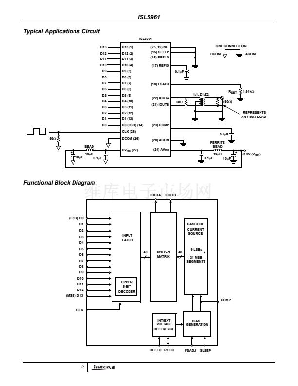
IOUTA and IOUTB are complementary current outputs. The
sum of the two currents is always equal to the full scale
output current minus one LSB. If single ended use is
desired, a load resistor can be used to convert the output
current to a voltage. It is recommended that the unused
output be either grounded or equally terminated. The voltage
developed at the output must not violate the output voltage
compliance range of -1.0V to 1.25V. R
OUT
(the impedance
loading each current output) should be chosen so that the
desired output voltage is produced in conjunction with the
output full scale current. If a known line impedance is to be
driven, then the output load resistor should be chosen to
match this impedance. The output voltage equation is:
V
OUT
= I
OUT
X R
OUT
.
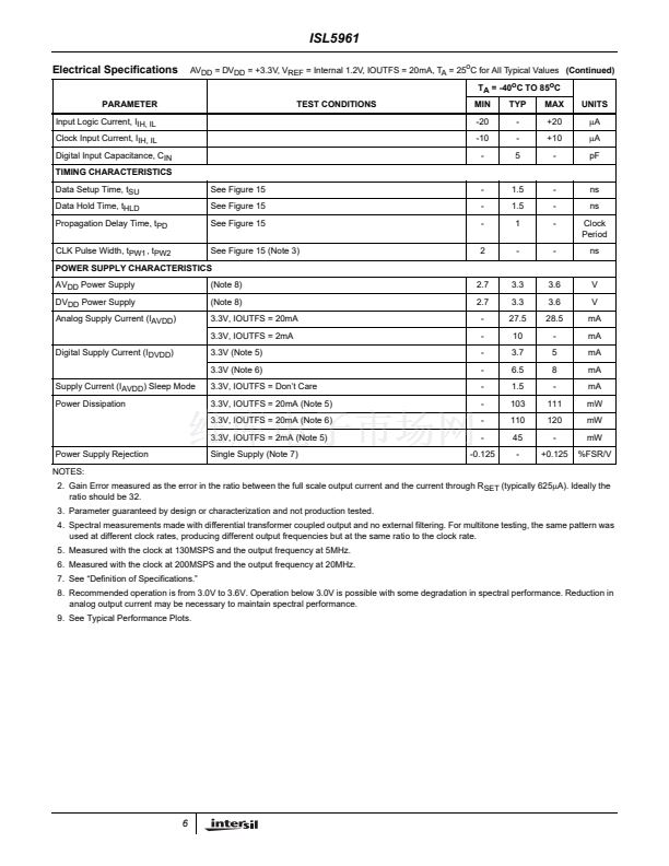
The most effective method for reducing the power
consumption is to reduce the analog output current, which
dominates the supply current. The maximum recommended
output current is 20mA.
Ground Planes
Separate digital and analog ground planes should be used.
All of the digital functions of the device and their
corresponding components should be located over the
digital ground plane and terminated to the digital ground
plane. The same is true for the analog components and the
analog ground plane.
Noise Reduction
To minimize power supply noise, 0.1碌F capacitors should be
placed as close as possible to the converter鈥檚 power supply
pins, AV
DD
and DV
DD
. Also, the layout should be designed
using separate digital and analog ground planes and these
capacitors should be terminated to the digital ground for
DV
DD
and to the analog ground for AV
DD
. Additional filtering
of the power supplies on the board is recommended.
Voltage Reference
The internal voltage reference of the device has a nominal
value of +1.23V with a
卤40ppm/
o
C drift coefficient over the
full temperature range of the converter. It is recommended
that a 0.1碌F capacitor be placed as close as possible to the
REFIO pin, connected to the analog ground. The REFLO pin
(16) selects the reference. The internal reference can be
selected if pin 16 is tied low (ground). If an external reference
is desired, then pin 16 should be tied high (the analog supply
voltage) and the external reference driven into REFIO, pin
17. The full scale output current of the converter is a function
of the voltage reference used and the value of R
SET
. I
OUT
should be within the 2mA to 20mA range, though operation
below 2mA is possible, with performance degradation.
If the internal reference is used, V
FSADJ
will equal
approximately 1.2V (pin 18). If an external reference is used,
V
FSADJ
will equal the external reference. The calculation for
I
OUT
(Full Scale) is:
I
OUT
(Full Scale) = (V
FSADJ
/R
SET)
X 32.
If the full scale output current is set to 20mA by using the
internal voltage reference (1.2V) and a 1.91k鈩?R
SET
resistor, then the input coding to output current will resemble
the following:
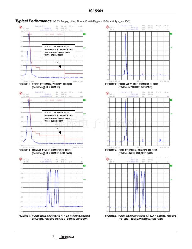
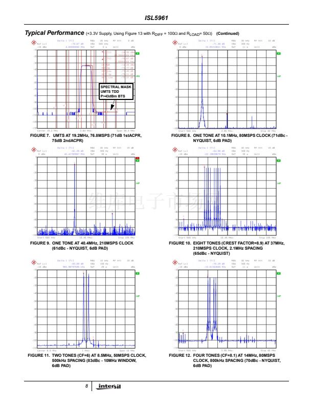
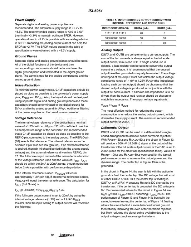
Differential Output
IOUTA and IOUTB can be used in a differential-to-single-
ended arrangement to achieve better harmonic rejection.
With R
DIFF
= 50鈩?and R
LOAD
=50鈩? the circuit in Figure 13
will provide a 500mV (-2.5dBm) signal at the output of the
transformer if the full scale output current of the DAC is set to
20mA (used for the electrical specifications table). Values of
R
DIFF
= 100鈩?and R
LOAD
=50鈩?were used for the typical
performance curves to increase the output power and the
dynamic range. The center tap in Figure 13 must be
grounded.
In the circuit in Figure 14, the user is left with the option to
ground or float the center tap. The DC voltage that will exist
at either IOUTA or IOUTB if the center tap is floating is
IOUT
DC
x (R
A
//R
B
) V because R
DIFF
is DC shorted by the
transformer. If the center tap is grounded, the DC voltage is
0V. Recommended values for the circuit in Figure 14 are
R
A
=R
B
=50鈩? R
DIFF
=100鈩? assuming R
LOAD
=50鈩? The
performance of Figure 13 and Figure 14 is basically the
same, however leaving the center tap of Figure 14 floating
allows the circuit to find a more balanced virtual ground,
theoretically improving the even order harmonic rejection,
but likely reducing the signal swing available due to the
output voltage compliance range limitations.
10


 1
1
 2
2
 3
3
 4
4
 5
5
 6
6
 7
7
 8
8
 9
9
 10
10
 11
11
 12
12
 13
13
