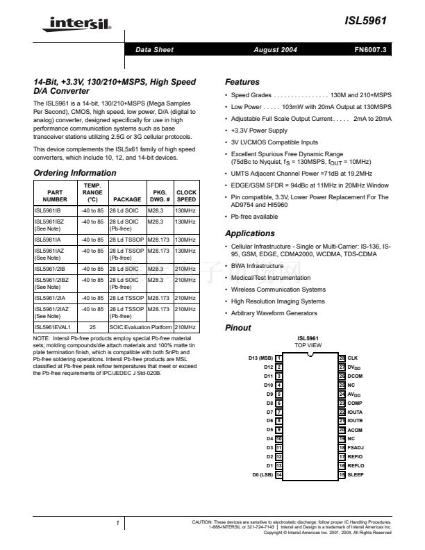
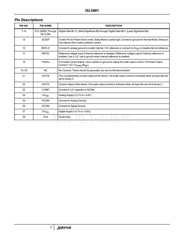
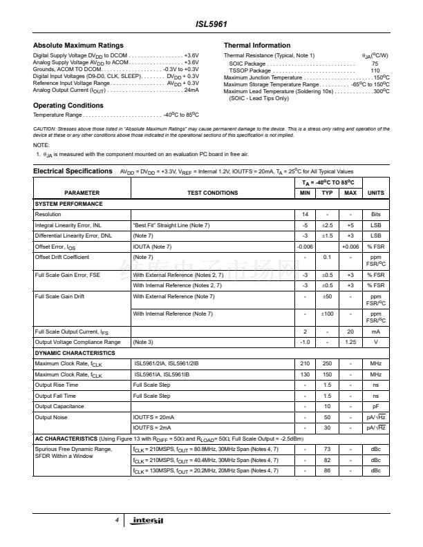
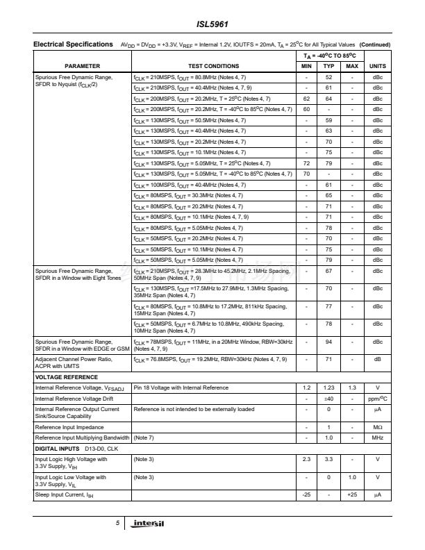
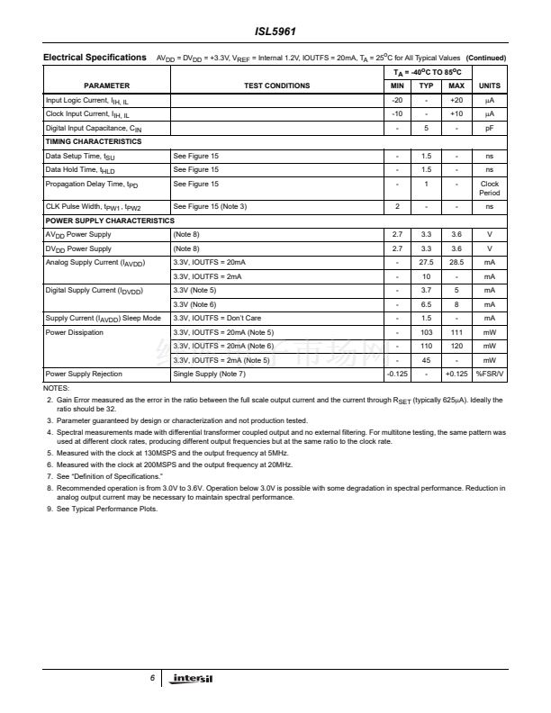
ISL5961
Definition of Specifications
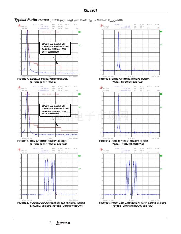
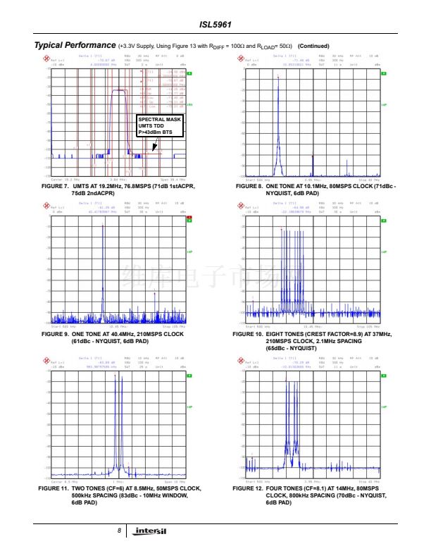
Adjacent Channel Power Ratio, ACPR,
is the ratio of the
average power in the adjacent frequency channel (or offset)
to the average power in the transmitted frequency channel.
Differential Linearity Error, DNL,
is the measure of the
step size output deviation from code to code. Ideally the step
size should be 1 LSB. A DNL specification of 1 LSB or less
guarantees monotonicity.
EDGE, Enhanced Data for Global Evolution,
a TDMA
standard for cellular applications which uses 200kHz BW, 8-
PSK modulated carriers.
Full Scale Gain Drift,
is measured by setting the data inputs
to be all logic high (all 1s) and measuring the output voltage
through a known resistance as the temperature is varied
from T
MIN
to T
MAX
. It is defined as the maximum
deviation
from the
value
measured at room temperature to the
value
measured at either T
MIN
or T
MAX
. The units are ppm of FSR
(full scale range) per
o
C.
Full Scale Gain Error,
is the error from an ideal ratio of 32
between the output current and the full scale adjust current
(through R
SET
).
GSM, Global System for Mobile Communication,
a TDMA
standard for cellular applications which uses 200kHz BW,
GMSK modulated carriers.
Integral Linearity Error, INL,
is the measure of the worst
case point that deviates from a best fit straight line of data
values along the transfer curve.
Internal Reference Voltage Drift,
is defined as the
maximum
deviation
from the
value
measured at room
temperature to the
value
measured at either T
MIN
or T
MAX
.
The units are ppm per
o
C.
Offset Drift,
is measured by setting the data inputs to all
logic low (all 0s) and measuring the output voltage at IOUTA
through a known resistance as the temperature is varied
from T
MIN
to T
MAX
. It is defined as the maximum
deviation
from the
value
measured at room temperature to the
value
measured at either T
MIN
or T
MAX
. The units are ppm of FSR
(full scale range) per degree
o
C.
Offset Error,
is measured by setting the data inputs to all
logic low (all 0s) and measuring the output voltage of IOUTA
through a known resistance. Offset error is defined as the
maximum
deviation
of the IOUTA output current from a value
of 0mA.
Output Voltage Compliance Range,
is the voltage limit
imposed on the output. The output impedance should be
chosen such that the voltage developed does not violate the
compliance range.
Power Supply Rejection,
is measured using a single power
supply. The nominal supply voltage is varied
卤
10% and the
change in the DAC full scale output is noted.
9
Reference Input Multiplying Bandwidth,
is defined as the
3dB bandwidth of the voltage reference input. It is measured
by using a sinusoidal waveform as the external reference
with the digital inputs set to all 1s. The frequency is
increased until the amplitude of the output waveform is 0.707
(-3dB) of its original value.
Spurious Free Dynamic Range, SFDR,
is the amplitude
difference from the fundamental signal to the largest
harmonically or non-harmonically related spur within the
specified frequency window.
Total Harmonic Distortion, THD,
is the ratio of the RMS
value of the fundamental output signal to the RMS sum of
the first five harmonic components.
UMTS, Universal Mobile Telecommunications System,
a
W-CDMA standard for cellular applications which uses
3.84MHz modulated carriers.
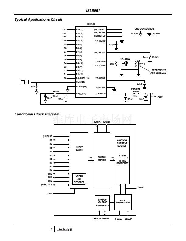
Detailed Description
The ISL5961 is a 14-bit, current out, CMOS, digital to analog
converter. The maximum update rate is at least 210+MSPS
and can be powered by a single power supply in the
recommended range of +3.0V to +3.6V. Operation with clock
rates higher than 210MSPS is possible; please contact the
factory for more information. It consumes less than 120mW
of power when using a +3.3V supply, the maximum 20mA of
output current, and the data switching at 210MSPS. The
architecture is based on a segmented current source
arrangement that reduces glitch by reducing the amount of
current switching at any one time. In previous architectures
that contained all binary weighted current sources or a
binary weighted resistor ladder, the converter might have a
substantially larger amount of current turning on and off at
certain, worst-case transition points such as midscale and
quarter scale transitions. By greatly reducing the amount of
current switching at these major transitions, the overall glitch
of the converter is dramatically reduced, improving settling
time, transient problems, and accuracy.
Digital Inputs and Termination
The ISL5961 digital inputs are guaranteed to 3V LVCMOS
levels. The internal register is updated on the rising edge of
the clock. To minimize reflections, proper termination should
be implemented. If the lines driving the clock and the digital
inputs are long 50鈩?lines, then 50鈩?termination resistors
should be placed as close to the converter inputs as possible
connected to the digital ground plane (if separate grounds
are used). These termination resistors are not likely needed
as long as the digital waveform source is within a few inches
of the DAC. For pattern drivers with very high speed edge
rates, it is recommended that the user consider series
termination (50-200鈩? prior to the DAC鈥檚 inputs in order to
reduce the amount of noise.


 1
1
 2
2
 3
3
 4
4
 5
5
 6
6
 7
7
 8
8
 9
9
 10
10
 11
11
 12
12
 13
13
