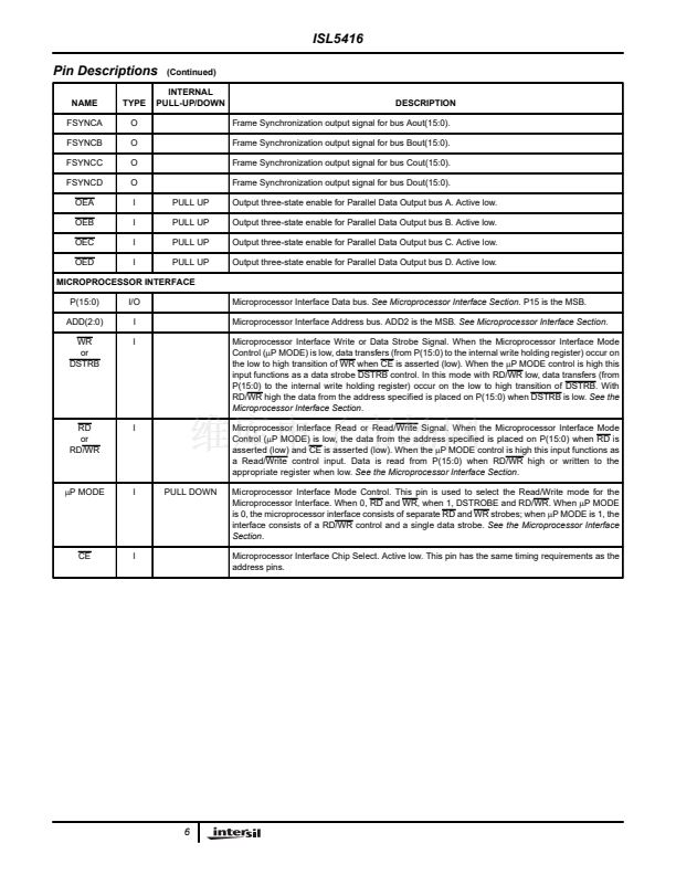
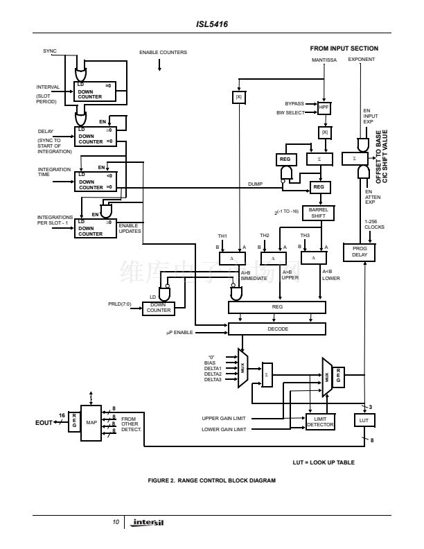
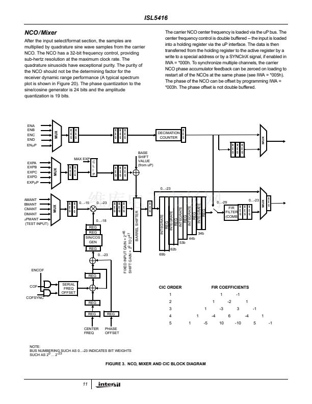
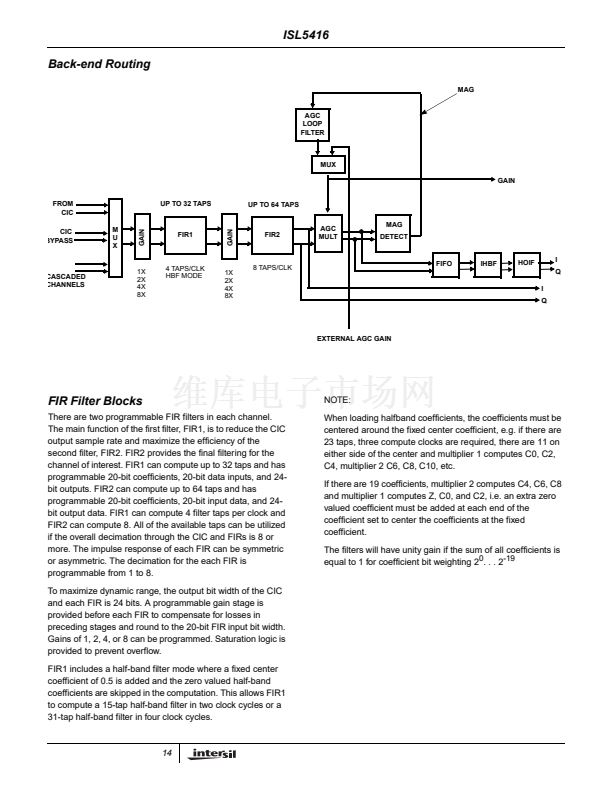
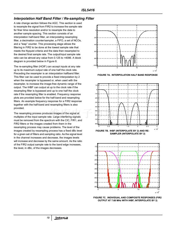
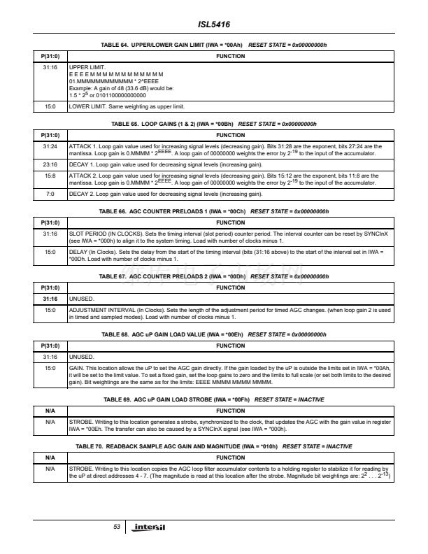
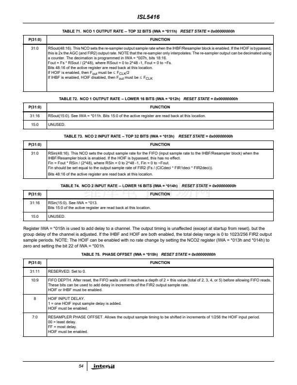
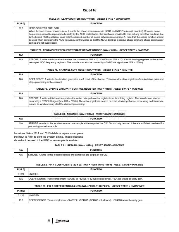
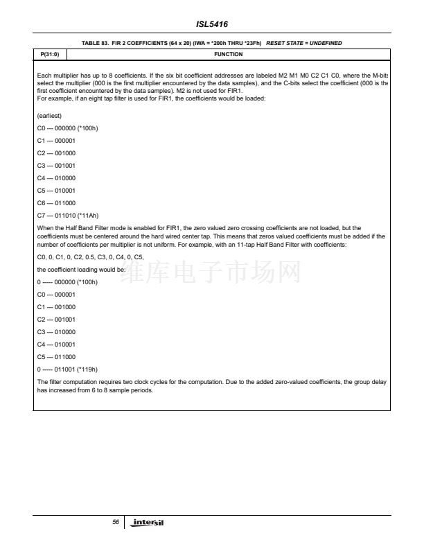
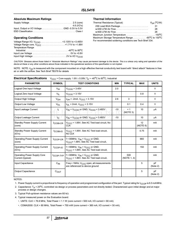
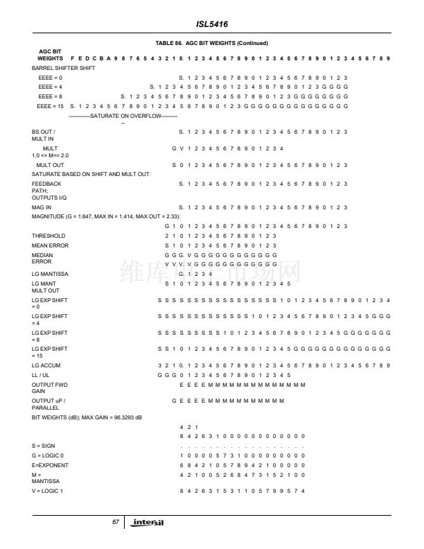
ISL5416
Tables of I/O Registers
TABLE 23.
CHANNEL INPUT FORMAT
(IWA = 0*00h)
RESET STATE = 0x00000000h
P(31:0)
31:16
15
14
13
UNUSED.
FIXED GAIN MODE IN VGA.
RESERVED. Set to 1.
INVERT INPUT CLOCK.
1 = High -> Low edge of the input clock samples input data.
0 = Low -> High edge of the input clock samples input data.
INPUT CLOCK SOURCE.
1 = CLKC
0 = CLKA for Ain (address 0000 XXX1 0000 0000)
CLKB for Bin (address 0000 XX1X 0000 0000)
CLKD for Din (address 0000 1XXX 0000 0000)
CLKC is always used for Cin
The rising edge of CLKC is always used for the channel processing and output timing.
INPUT FORMAT.
1 = offset binary.
0 = 2鈥檚 complement
GATED & INTERPOLATED.
1 = input interpolated.
0 = input gated.
DEMUX DELAY.
000 = no delay, take sample aligned with the enable.
111 = take 7th sample after the enable.
RESERVED. Set to 0.
LSB TO MSB SWAP ON DATA.
1 = input bus reversed MSB for LSB -- XIN(0) = MSB.
0 = input bus normal XIN(16) = MSB
Provided to simplify circuit board routing.
FIXED/FLOATING POINT MODE.
00 = 16-bit fixed point (bits 16:1, 0 unused).
01 = 14/3 floating point (bits 16:3 mantissa, 2:0 exponent).
10 = 15/2 floating point (bits 16:2 mantissa, 1:0 exponent).
11 = 16/1 floating point (bits 16:1 mantissa, 0 exponent).
RESERVED. Set to 0.
FUNCTION
12
11
10
9:7
6:5
4
3:2
1:0
36


 1
1
 2
2
 3
3
 4
4
 5
5
 6
6
 7
7
 8
8
 9
9
 10
10
 11
11
 12
12
 13
13
 14
14
 15
15
 16
16
 17
17
 18
18
 19
19
 20
20
 21
21
 22
22
 23
23
 24
24
 25
25
 26
26
 27
27
 28
28
 29
29
 30
30
 31
31
 32
32
 33
33
 34
34
 35
35
 36
36
 37
37
 38
38
 39
39
 40
40
 41
41
 42
42
 43
43
 44
44
 45
45
 46
46
 47
47
 48
48
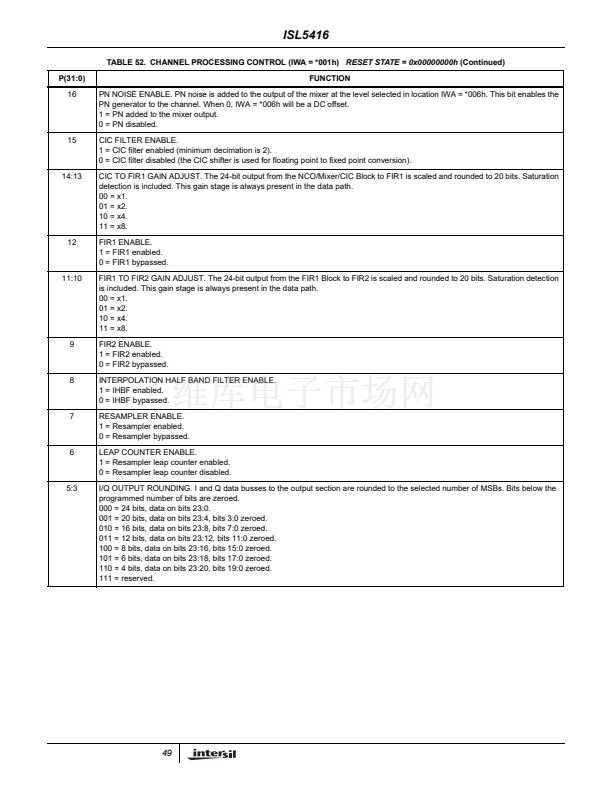 49
49
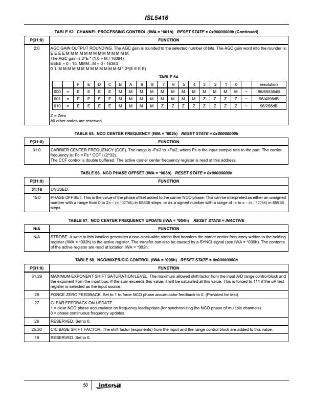 50
50
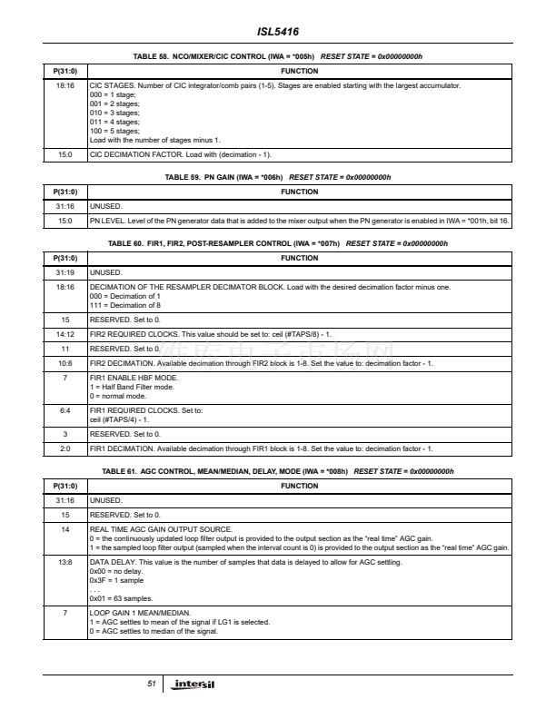 51
51
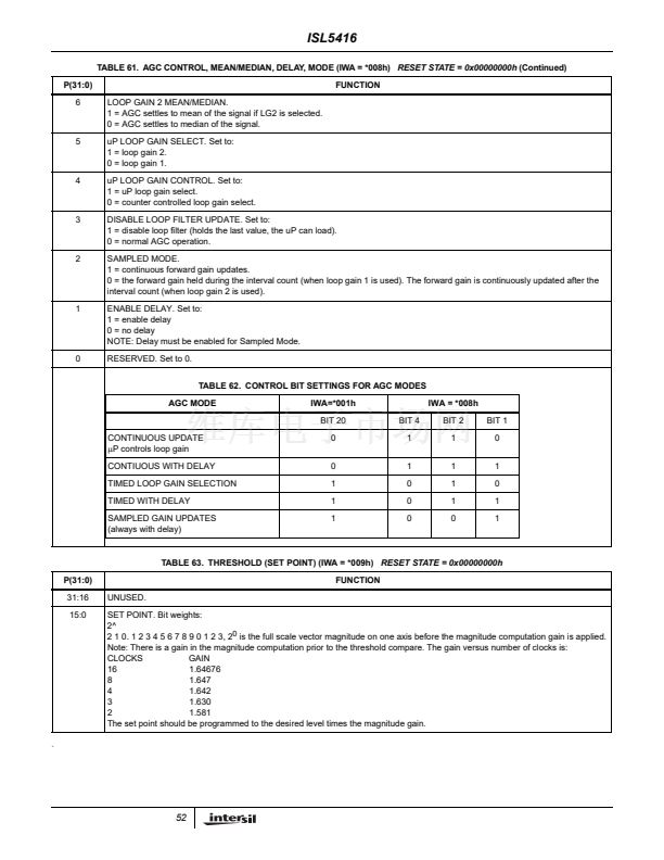 52
52
 53
53
 54
54
 55
55
 56
56
 57
57
 58
58
 59
59
 60
60
 61
61
 62
62
 63
63
 64
64
 65
65
 66
66
 67
67
 68
68
 69
69
 70
70
 71
71
