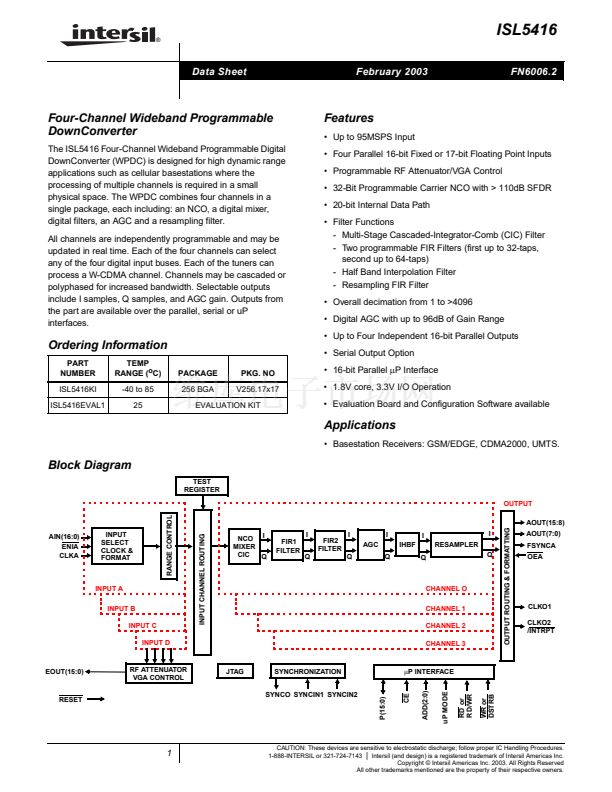
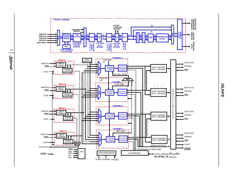
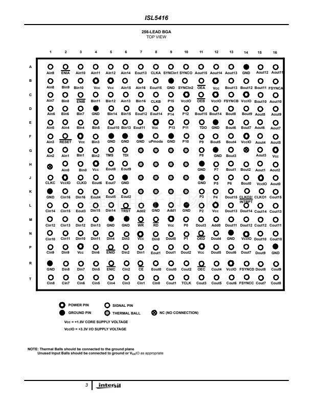
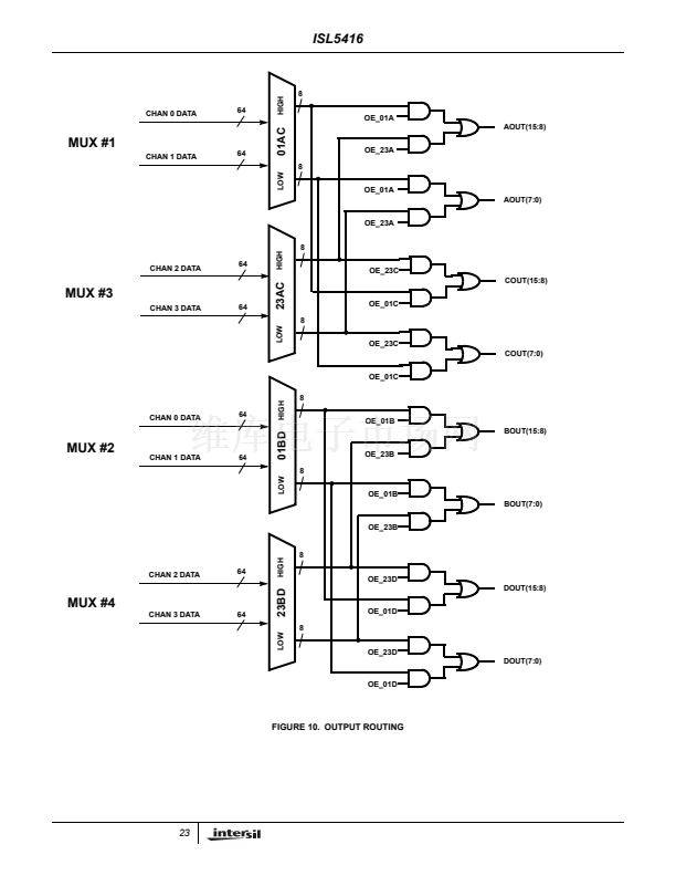
ISL5416
Pin Descriptions
NAME
TYPE
INTERNAL
PULL-UP/DOWN
DESCRIPTION
POWER SUPPLY
Vcc
VccIO
GND
INPUTS
Ain(16:0)
I
PULL DOWN
Parallel Data Input bus A. Sampled on the rising or falling edge (programmable) of clock when ENIA
is active (low). The bus order can be programmed (See IWA = 0*00h, bit 4).
Parallel Data Input bus B. Sampled on the rising or falling edge (programmable) of clock when ENIB
is active (low). The bus order can be programmed (See IWA = 0*00h, bit 4).
Parallel Data Input bus C. Sampled on the rising or falling edge (programmable) of clock when ENIC
is active (low). The bus order can be programmed (See IWA = 0*00h, bit 4).
Parallel Data Input bus D. Sampled on the rising or falling edge (programmable) of clock when ENID
is active (low). The bus order can be programmed (See IWA = 0*00h, bit 4).
Input enable for Parallel Data Input bus A. Active low. This pin enables the input to the part in one of
two modes, gated or interpolated. In gated mode, one sample is taken per CLK when ENIx is
asserted.
Input enable for Parallel Data Input bus B. Active low. This pin enables the input to the part in one of
two modes, gated or interpolated. In gated mode, one sample is taken per CLK when ENIx is
asserted.
Input enable for Parallel Data Input bus C. Active low. This pin enables the input to the part in one of
two modes, gated or interpolated. In gated mode, one sample is taken per CLK when ENIx is
asserted.
Input enable for Parallel Data Input bus D. Active low. This pin enables the input to the part in one of
two modes, gated or interpolated. In gated mode, one sample is taken per CLK when ENIx is
asserted.
-
-
-
Positive Power Supply Voltage (core), 1.8V
卤0.09
Positive Power Supply Voltage (I/O), 3.3V
卤0.165
Ground, 0V.
Bin(16:0)
I
PULL DOWN
Cin(16:0)
I
PULL DOWN
Din(16:0)
I
PULL DOWN
ENIA
I
PULL DOWN
ENIB
I
PULL DOWN
ENIC
I
PULL DOWN
ENID
I
PULL DOWN
CONTROL
CLKA
CLKB
CLKC
CLKD
SYNCIn1
I
I
I
I
I
PULL DOWN
PULL DOWN
PULL DOWN
PULL DOWN
Input clock for data bus A. CLKA or CLKC may be used for Ain(16:0).
Input clock for data bus B. CLKB or CLKC may be used for Bin(16:0).
Input clock for data bus C. CLKC is also the master clock for all channels of ISL5416
Input clock for data bus D. CLKD or CLKC may be used for Din(16:0).
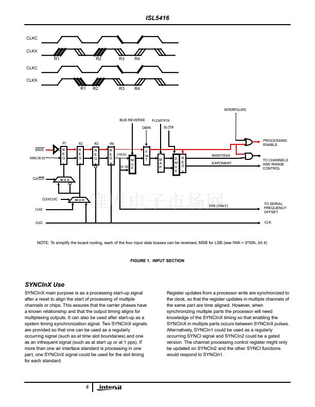
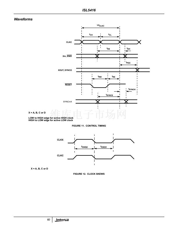
Global synchronization input signal 1. SYNCIn1 can update the carrier NCOs, reset decimation
counters, restart the filter, and restart the output section among other functions. For most of the
functional blocks, the response to SYNCIn1 is programmable and can be enabled or disabled.
Global synchronization input signal 2. SYNCIn2 can update the carrier NCOs, reset decimation
counters, restart the filter, and restart the output section among other functions. For most of the
functional blocks, the response to SYNCIn2 is programmable and can be enabled or disabled.
Synchronization Output Signal. The processing of multiple ISL5416 devices can be synchronized by
tying the SYNCO from one ISL5416 device (the master) to the SYNCIn of all the ISL5416 devices
(the master and slaves). An optional internal SYNCO to SYNCInX connection is provided.
PULL UP
Reset Signal. Active low. Asserting reset will halt all processing and set certain registers to default
values.
SYNCIn2
I
PULL DOWN
SYNCO
O
RESET
I
4


 1
1
 2
2
 3
3
 4
4
 5
5
 6
6
 7
7
 8
8
 9
9
 10
10
 11
11
 12
12
 13
13
 14
14
 15
15
 16
16
 17
17
 18
18
 19
19
 20
20
 21
21
 22
22
 23
23
 24
24
 25
25
 26
26
 27
27
 28
28
 29
29
 30
30
 31
31
 32
32
 33
33
 34
34
 35
35
 36
36
 37
37
 38
38
 39
39
 40
40
 41
41
 42
42
 43
43
 44
44
 45
45
 46
46
 47
47
 48
48
 49
49
 50
50
 51
51
 52
52
 53
53
 54
54
 55
55
 56
56
 57
57
 58
58
 59
59
 60
60
 61
61
 62
62
 63
63
 64
64
 65
65
 66
66
 67
67
 68
68
 69
69
 70
70
 71
71
