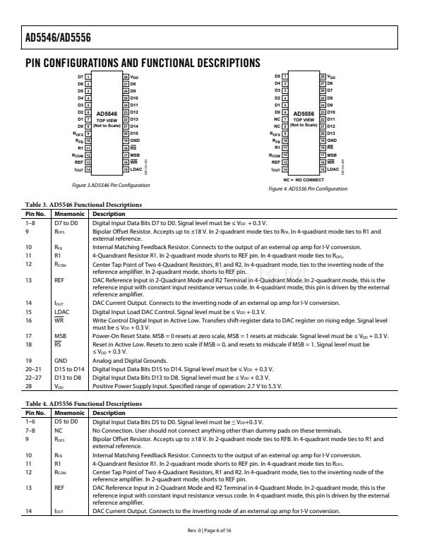
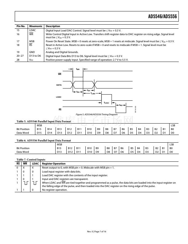
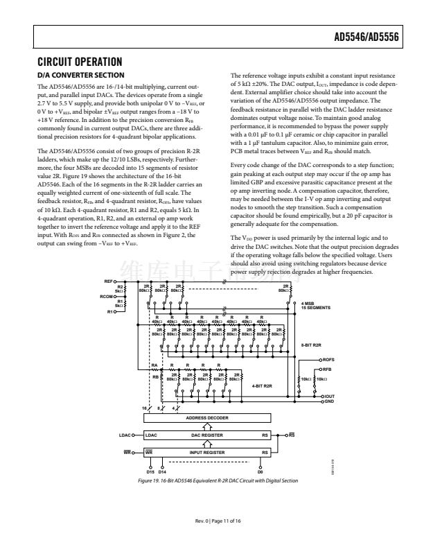
AD5546/AD5556
APPLICATIONS
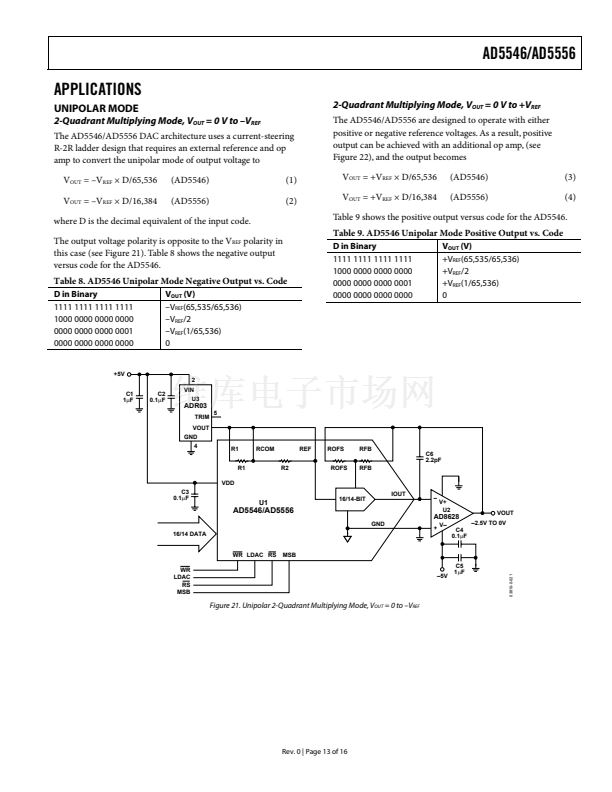
UNIPOLAR MODE
2-Quadrant Multiplying Mode, V
OUT
= 0 V to 鈥揤
REF
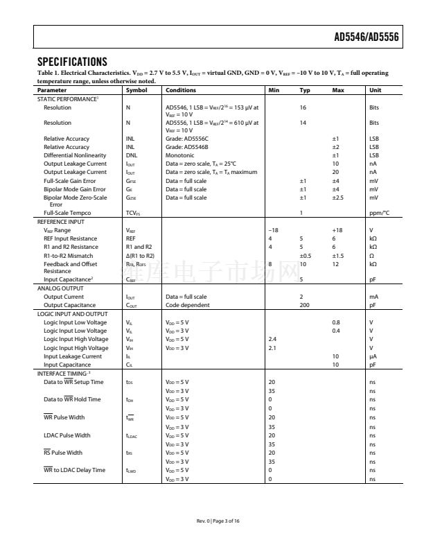
The AD5546/AD5556 DAC architecture uses a current-steering
R-2R ladder design that requires an external reference and op
amp to convert the unipolar mode of output voltage to
V
OUT
= 鈥揤
REF
脳 D/65,536
V
OUT
= 鈥揤
REF
脳 D/16,384
(AD5546)
(AD5556)
(1)
(2)
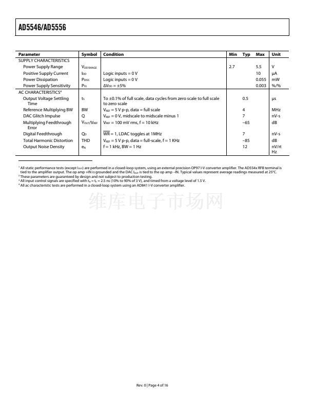
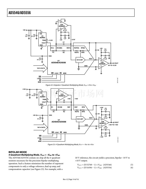
2-Quadrant Multiplying Mode, V
OUT
= 0 V to +V
REF
The AD5546/AD5556 are designed to operate with either
positive or negative reference voltages. As a result, positive
output can be achieved with an additional op amp, (see
Figure 22), and the output becomes
V
OUT
= +V
REF
脳 D/65,536
V
OUT
= +V
REF
脳 D/16,384
(AD5546)
(AD5556)
(3)
(4)
where D is the decimal equivalent of the input code.
The output voltage polarity is opposite to the V
REF
polarity in
this case (see Figure 21). Table 8 shows the negative output
versus code for the AD5546.
Table 8. AD5546 Unipolar Mode Negative Output vs. Code
D in Binary
1111 1111 1111 1111
1000 0000 0000 0000
0000 0000 0000 0001
0000 0000 0000 0000
V
OUT
(V)
鈥揤
REF
(65,535/65,536)
鈥揤
REF
/2
鈥揤
REF
(1/65,536)
0
Table 9 shows the positive output versus code for the AD5546.
Table 9. AD5546 Unipolar Mode Positive Output vs. Code
D in Binary
1111 1111 1111 1111
1000 0000 0000 0000
0000 0000 0000 0001
0000 0000 0000 0000
V
OUT
(V)
+V
REF
(65,535/65,536)
+V
REF
/2
+V
REF
(1/65,536)
0
+5V
C1
1碌F
C2
0.1碌F
2
VIN
U3
ADR03
TRIM
VOUT
GND
4
R1
R1
5
RCOM
R2
REF
ROFS
ROFS
RFB
RFB
C6
2.2pF
VDD
C3
0.1碌F
AD5546/AD5556
GND
16/14 DATA
WR LDAC RS
WR
LDAC
RS
MSB
MSB
U1
16/14-BIT
IOUT
鈥?/div>
AD8628
+
V鈥?/div>
C4
0.1碌F
V+
U2
VOUT
鈥?.5V TO 0V
Figure 21. Unipolar 2-Quadrant Multiplying Mode, V
OUT
= 0 to 鈥揤
REF
Rev. 0 | Page 13 of 16
03810-0-021
鈥?V
C5
1碌F


 1
1
 2
2
 3
3
 4
4
 5
5
 6
6
 7
7
 8
8
 9
9
 10
10
 11
11
 12
12
 13
13
 14
14
 15
15
 16
16
